Overview
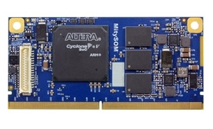
The MitySOM-5CSx is a family of highly-configurable, small form-factor System on Module (SOM) designed for high-throughput applications requiring single or dual hard-core Cortex-A9 applications processors tightly integrated with FPGA fabric. The MitySOM-5CSx combines the Altera Cyclone V System on Chip (SoC), memory subsystems and onboard power supplies. The MitySOM-5CSx provides a complete and flexible CPU and FPGA infrastructure for highly-integrated embedded systems.
This SOM features a Hard Processor System (HPS) providing up to 4,000 MIPS at speeds of up to 925 MHz per core and is combined with a NEON coprocessor with double-precision FPU (one per core). The MitySOM-5CSx combines a Cyclone V with up to 2GB of DDR3 CPU/FPGA RAM with ECC, 512MB of dedicated DDR3 FPGA RAM (optional) and up to 48MB of QSPI NOR Flash creating a high-bandwidth system for embedded applications. The ARM architecture supports several high level operating systems, including Embedded Linux, Micrium uC/OS, Android, QNX, and Windows Embedded Compact.
By combining six 3.125Gbps transceivers, one PCIe hard core, up to 133 user I/O, and dual Gigabit Ethernet interfaces, the system can simultaneously acquire and efficiently process large amounts of data.
The MitySOM-5CSx has been designed to support several upgrade options. These include various speed grades, memory configurations, and operating temperature specifications (including commercial and industrial temperature ranges).
Applications
- Machine Vision
- Scientific Imaging
- Motor Control
- Medical Imaging
- Medical Instrumentation
- Test and Measurement
- Industrial Instrumentation
- Military/Aerospace
Documentation
Specifications
CPU
| Cortex-A9 Applications Processor(s) | |
| Max # of Cores | 2 |
| Max CPU Speed | 925MHz |
| L1 Program Cache | 32KB |
| L1 Data Cache | 32KB |
| L2 Cache | 512KB |
| Internal RAM | 64KB |
CPU subsystem is a hard IP block referred to by Altera as the HPS, Hard Processor Subsystem
Memory
| System Memory | |
| Max RAM* | 2GB DDR3 with ECC |
| Max FPGA Private RAM | 512MB DDR3 |
| NOR Flash | Up To 48MB |
* RAM is accessible from the Cortex-A9 application processor(s) and the FPGA fabric
| FPGA Fabric | |
| Max Logic Elements | 110kLE |
| Global Clock | 460MHz |
| Max M10K Memory | 5.1Mb |
| Max MLAB Memory | 621Kb |
| Max DSP Blocks | 112 |
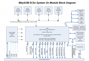
Block Diagram
Interfaces
| 2 Gigabit Ethernet | 2 UARTs | 2 SPI Master |
| 6 High speed transceivers, 3.125Gbps | 1 MMC/SD/SDIO | 2 SPI Slave |
| High speed serializers | 2 USB 2.0 OTG | 4 I2C |
| PCIe Hard IP Block | 2 CAN | 3 HPS PLLs |
| Max 133 Direct FPGA I/Os |
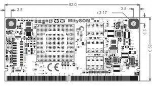
Mechanical
Development Kits
Development Tools and Software
Software Support
- Embedded Linux
- Wind River VxWorks
- Windows Embedded Compact
- QNX
- Android
- Qt Embedded Graphics
- Micrium uC/OS
Development Tools
- Quartus Prime Standard
- GNU Toolchain
- Terasic USB Blaster
Technical Support
Our customers benefit from engineering and applications support for the life of their product. This includes free, lifetime access to our technical support site, as well as access to application engineering resources and other services.
- Visit our MitySOM-5CSx Altera Cyclone V Wiki to access:
- Linux OS and board support package details, including source code
- Product change notices
- Base board design guide
- Development kit base board design files
- Software guide to getting started, tool chain, tips and how-to’s
- Hardware power draw, pin outs, shock and vibration, CAD files, mechanical drawings and 3D models
- Frequently asked questions
- Visit our MitySOM-5CSx Altera Cyclone V Forum to access:
- Software, Hardware, and FPGA forums
- Altera Cyclone V SoC Information
Critical Link’s embedded design team also offers engineering services and other support options such as:
- Schematic design review for customer designed carrier boards
- Complete design review services
- Software development services, including custom BSP development
- Base board development services
- Systems Engineering, Software, and Hardware Design to support your project anywhere in the product development lifecycle
Contact us for more information on these services.
Video
Related Products
Purchase
| Module P/N | Cores | FPGA I/O |
Speed Grade |
FPGA RAM |
FPGA KLE |
HPS RAM |
NOR | Temp | Buy |
| 5CSE-L2-3Y8-RC | Single | 133 | 8 | N/A | 25 | 512MB | 16MB | 0C to 70C | Buy |
| 5CSE-H4-3YA-RC | Dual | 133 | 7 | N/A | 40 | 1GB with ECC | 16MB | 0C to 70C | Buy |
| 5CSE-H4-3YA-RI | Dual | 133 | 7 | N/A | 40 | 1GB with ECC | 16MB | -40C to 85C | Buy |
| 5CSX-H5-4YA-RC | Dual | 133 | 7 | N/A | 85 | 1GB with ECC | 32MB | 0C to 70C | Buy |
| 5CSX-H5-4YA-RI | Dual | 133 | 7 | N/A | 85 | 1GB with ECC | 32MB | -40C to 85C | Buy |
| 5CSX-H6-42A-RC | Dual | 107 | 7 | 256MB | 110 | 1GB with ECC | 32MB | 0C to 70C | Buy |
| 5CSX-H6-42A-RI | Dual | 107 | 7 | 256MB | 110 | 1GB with ECC | 32MB | -40C to 85C | Buy |
| 5CSX-H6-4YA-RC | Dual | 133 | 7 | N/A | 110 | 1GB with ECC | 32MB | 0C to 70C | Buy |
| 5CSX-H6-4YA-RI | Dual | 133 | 7 | N/A | 110 | 1GB with ECC | 32MB | -40C to 85C | Buy |
| 5CSX-H6-53B-RC | Dual | 107 | 7 | 512MB | 110 | 2GB with ECC | 48MB | 0C to 70C | Buy |
Does your application require an even more rugged version of the SoC-based SOM? Contact Critical Link to learn about available options.
Find your local sales contact.
*Note: The selected distributor does not yet carry this model. You may contact them for ordering information, or submit a request directly to Critical Link.

MitySOM-5CSx System on Module
Get this product directly from Critical Link:
Or click to order this product from one of our distributors:


