Syracuse, N.Y. – April 30, 2024– Critical Link, LLC, a leading US-based manufacturer of FPGA, DSP, and CPU-based System on Modules, is pleased to announce new embedded solutions around the AgilexTM 5 SoC FPGA E-Series from Altera®. Critical Link is developing two product families around the Agilex 5 SoC FPGA E-Series: a single board computer and a system on module (SOM) family.
The MitySBC-A5E single-board computer was developed as part of the Agilex 5 SoC FPGA Early Access Program and will be the first to market. The MitySBC-A5E features a 32mm x 32mm Agilex 5 SoC FPGA E-Series with 656K LE FPGA fabric, dual-core Cortex-A55, dual-core Cortex-A76, PCIe 3.0, and 24 transceivers up to 17Gbps. The board includes 8GB LPDDR4 for the HPS, 8GB LPDDR4 for the FPGA, 64GB eMMC, microSD, and QSPI NOR for configuration. A rich set of interfaces, including 8 MIPI x4 lanes, 2.5G Ethernet, FMC, USB-C & USB 2, among others, make this a powerful solution for embedded product development teams working on next-generation industrial performance applications.
The MitySBC-A5E will be available as a development kit as well as a production-suitable single-board computer for customers interested in achieving first-to-market advantages with the high-performance, low-power Agilex 5 SoC FPGA. The product datasheet and other documentation are available today, and customers will benefit from Critical Link’s engineering and application support for the life of their product.
“Critical Link has been partnering with Altera and Intel for more than 10 years, helping customers reach the market fast with next-generation products based on the latest FPGA technology,” says Tom Catalino, Vice President and Founder of Critical Link, LLC. “We are excited to lead the next wave of FPGA-based designs and bring the Agilex 5 SoC FPGA power and performance advantages to our customers.”
Following the introduction of the single board computer, Critical Link is bringing the MitySOM®-A5E family of system-on-modules to market later this year. The MitySOM-A5E family will offer a wide range of FPGA densities, memory configurations, optional transceivers, and temperature ranges all in a compact 51mm x 71mm (2.0” x 2.8”) form factor to fit most applications. These modules are designed for long-term availability and support, meaning customers can confidently design them into long lifespan products in the test & measurement, medical/scientific, defense, and energy/utilities industries.
Prototypes for the MitySBC-A5E will be available in Q2 2024, with production in early 2025. System on Module prototypes are expected later this year with production to start in 2025.
Critical Link, LLC(Syracuse, NY www.criticallink.com), founded in 1997, develops system on modules (SOMs) for electronic applications. Our MitySOM® and MityDSP® families incorporate the latest FPGA, DSP, and CPU technologies, and are designed for long product lifespan and performance in the field. We supply OEMs in a wide range of industries including manufacturing, medical, scientific, defense, and energy/utilities. We ship worldwide and are franchised with many of the top electronics distributors.
Critical Link, LLC, is privately held and is ISO 9001:2015 Registered by SRI Quality System Registrar. Critical Link is a Gold-level member of the Intel® Partner Alliance.
*Altera Agilex 5 FPGA D-series (A5D031, mid-speed grade) vs. AMD/Xilinx Versal (VM1102, -3HS speed grade) at 90% utilization, 600-Mhz, using vendors power estimator calculators.
Altera, the Altera logo, and other Altera marks are trademarks of Altera or its subsidiaries.
“The customers who come to Senseeker are also often looking for other specialist electronics, and that’s where Critical Link fits in. They have a reputation for quality, and a long track record of working with complex applications. We wanted them to be part of our ecosystem,” — Ross Bannatyne, Senseeker Director of Business Development
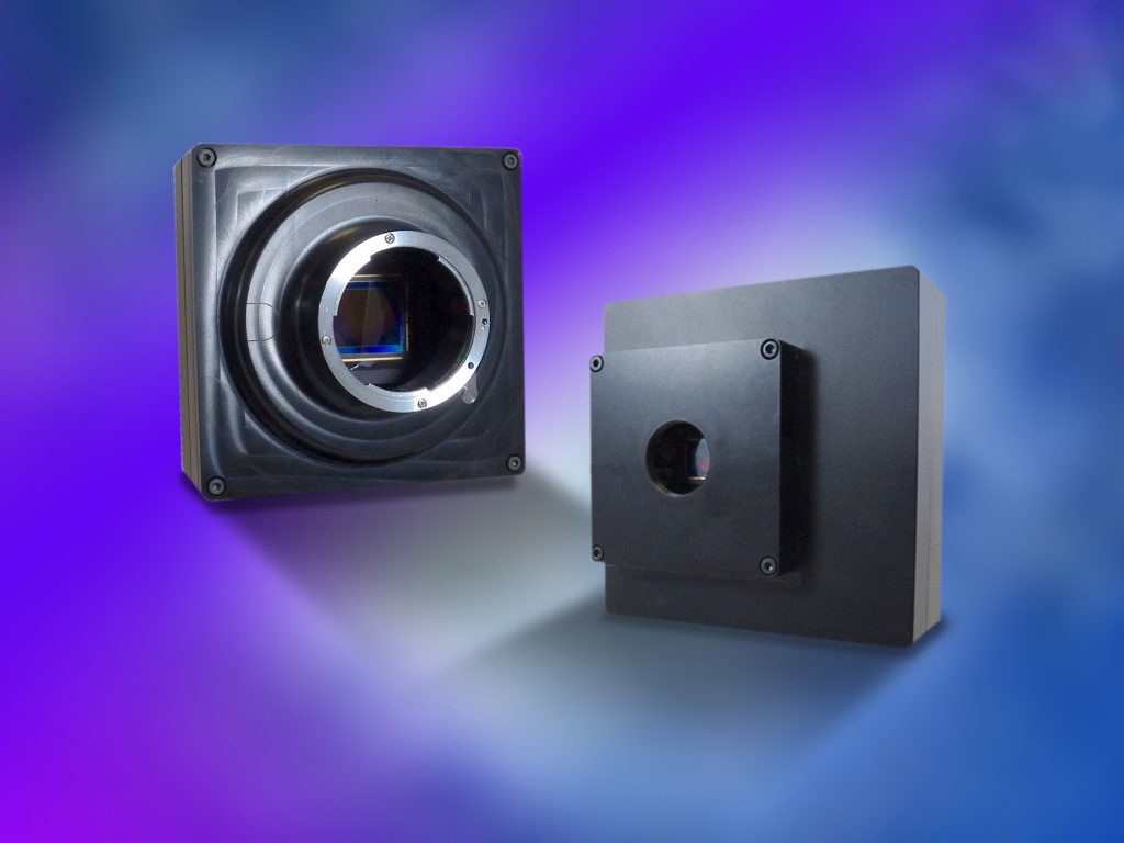
When Senseeker approached Critical Link about partnering, Critical Link was more than interested. Senseeker specializes in infrared image sensing products and services. Their state-of-the-art digital imaging sensors and readout integrated circuits for hybrid infrared image sensing arrays are used in cutting-edge security, military, and machine vision applications – the types of application where Critical Link technology is often embedded.
For Critical Link, working with Senseeker would be a partnership with a twist. Critical Link’s traditional partnerships have been formed with technology providers whose hardware and software are integral to the company’s System on Modules (SOMs). With Senseeker, Critical Link would be providing a key component of the Evaluation Kits for their Oxygen® RD0092, an off-the-shelf digital readout IC (DROIC) and Magnesium® MIL RP0092 digital pixel readout IC (DPROIC).
Critical Link provides key technology
Senseeker’s Oxygen® RD0092 is the world’s first 8 μm pitch dual-band DROIC, providing infrared image system developers access to state-of-the-art technology without incurring the cost and risk associated with ground-up, custom designs. Used in defense and security applications such as infrared search and track and situation awareness, the Oxygen RD0092 is available to developers off-the-shelf in wafer form and is supported with an Evaluation Kit that expedites the infrared image sensing development cycle.
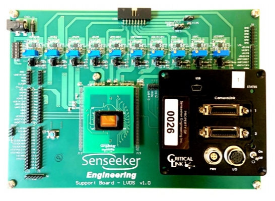
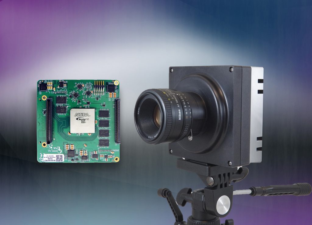
The Evaluation Kit includes an image acquisition support board from Critical Link, an engineering firm that develops embedded solutions for a wide range of electronic applications. The Critical Link support board captures high-speed digital data acquired from the Senseeker readout IC, converts it for use, and transmits it for display to a host PC containing a commercial frame grabber card. The image acquisition support board that makes up part of the Evaluation Kit is based on Critical Link’s MitySOM-5CSx, a highly-configurable small form-factor System on Module (SOM). The MitySOM-5CSx is designed for high-throughput applications requiring single or dual hard-core Cortex-A9 applications processors tightly integrated with FPGA fabric. The MitySOM-5CSx combines the Altera Cyclone V System on Chip (SoC), memory subsystems and onboard power supplies, including two Camera Link ports. The MitySOM-5CSx provides a complete and flexible CPU and FPGA infrastructure for highly-integrated embedded systems.
The image acquisition support board is designed to be supplied by an external 5V supply, and provides adjustable detector bias voltages. It also includes connections for an optional external clock input, as well as numerous digital and analog test points. The board supports both room temperature (uncooled) and cryogenic (cooled) evaluation.
For Senseeker, a partnership that makes sense
Ross Bannatyne is Senseeker’s Director of Business Development. “The customers who come to Senseeker are also often looking for other specialist electronics, and that’s where Critical Link fits in. They have a reputation for quality, and a long track record of working with complex applications. We wanted them to be part of our ecosystem,” Bannatyne says. Senseeker is currently transitioning from a pure custom-design producer to a company that offers both custom design and custom-off-the-shelf products. “When we first began talking with Critical Link, we found that, many years ago, they’d also made this type of transition, so it’s an especially good match. Critical Link just gets us.”
A shared set of core values
“We’re excited to be partnering with Senseeker,” says Tom Catalino, co-Founder and Vice President of Critical Link. “Early on in our discussions, we realized that we not only shared a passion for electronics, but that our core values are in sync. We’re both committed to excellence, and to making it possible for our clients to accelerate product development without having to sacrifice on quality, cost, or the ability to easily make the customizations that that make their products unique.”
About Critical Link
Syracuse, NY-based Critical Link (www.criticallink.com) is an embedded systems engineering firm, offering a broad range of customizable SOMs and cameras for industrial performance applications. Critical Link’s end-to-end product engineering offerings include design, development, and production services. The company’s expertise in image sensor integration, system-on-chip (SoC) and field-programmable gate array (FPGA) designs, vision protocols, and signal processing has made it a leader in board-level solutions and custom designs for OEMs and embedded developers around the world. Privately held, Critical Link is a Platinum member of the Intel FPGA Design Services Network and Intel IoT Solutions Alliance, a Platinum member of the Texas Instruments Design Network, and is ISO 9001:2015 Registered by SRI Quality System Registrar.
Syracuse, N.Y. – The JESD204B serial interface has become the interface standard of choice for high-speed analog-to-digital and digital-to-analog converters (ADCs and DACs). Intel® FPGAs and Intel® SOC FPGAs are well suited to interface to these converters using this interface and Arrow Electronics™ has developed four JESD204B reference solutions using high-speed analog RF transceivers and converter modules based on Analog Devices RF transceivers, ADCs, and DACs. These solutions employ third party carrier board platforms from Critical Link supporting production-ready Systems on Modules (SOMs) based on Intel® Arria® 10 SOC FPGAs.
The hardware for each of these platforms includes:
An Intel Arria 10 SoC FPGA SOM
A carrier card with an FMC HPC connector
An Analog Devices FMC converter board
Example reference designs for the platforms include:
JESD204B HDL code for the Intel Arria 10 SoC FPGA
Bootable Linux operating system image
Custom IIO Linux device drivers
Support for IIO Oscilloscope, an Analog Devices developed Linux user space application
Each reference platform also includes a unique Quick Start Guide and complete source code for an example design. All documentation is now freely available on GitHub.
The four Arrow Electronics reference platforms are:
The ADRV9371 Platform: The ADRV9371 Platform is a complete development platform for applications that require high-performance radios capable of operating over a wideband frequency range. This platform is based on the Analog Devices AD9371 dual RF transceiver, which has a tunable range of 300 MHz to 6000 MHz. The ADRV9371 FMC converter evaluation board connects to the Intel Arria 10 SoC FPGA using the JESD204B serial interface over an FMC connector at lane rates as high as 6.144 Gbps.
The ADRV9375 Platform: Similar to the ADRV9371 Platform, the ADRV9375 Platform connects an Intel Arria 10 SoC FPGA to an ADRV9375 evaluation board through an FMC connector using a JESD204B serial interface operating at lane rates as high as 6.144 Gbps. The Analog Devices ADRV9375 evaluation board is based on the Analog Devices AD9375 dual RF transceiver, which is similar to the Analog Devices AD9371 dual RF transceiver, but the AD9375 dual RF transceiver adds an on-chip digital pre-distortion (DPD) algorithm block.
The AD-FMCDAQ2 Platform: This platform connects an Intel Arria® 10 SoC FPGA to an AD-FMCDAQ2 evaluation board over an FMC connector using the JESD204B serial interface operating at lane rates as high as 6.144 Gbps. The AD-FMCDAQ2 evaluation board incorporates an Analog Devices AD9144 high-speed DAC and an Analog Devices AD9680 high-speed ADC.
The ADRV9371, ADRV9375, and AD-FMCDAQ2 reference platforms are ideal for developing a wide range of RF applications including:
3G/4G micro and macro base stations
3G/4G multicarrier picocells
FDD and TDD antenna systems
Microwave NLOS backhaul systems
Test and measurement applications
Software defined radios (SDR)
The ADRV9009 Platform: This platform connects an Intel Arria® 10 SoC FPGA to an Analog Devices ADRV9009 evaluation board over an FMC connector using the JESD204B serial interface operating at lane rates as high as 12.288 Gbps. The Analog Devices’ ADRV9009 is a wide bandwidth, high performance RF integrated transceiver with dual transmitters; dual receivers; and a dual-input, shared-observation receiver. This platform is ideal for developing a wide range of RF applications including:
3G/4G/5G TDD Macro Cell Base Stations
TDD Active Antenna Systems
Massive MIMO
Phased Array Radar
Electronic Warfare
Military Communications
Portable Test Equipment
Loaner kits are available from Arrow Electronics for customers to evaluate these solutions. Please contact your local Arrow rep for more information.
Article provided courtesy of Intel, original post: https://blogs.intel.com/psg/arrow-electronics-develops-a-series-of-four-complete-rf-reference-platforms-based-on-the-intel-arria-10-soc-fpga-and-analog-devices-high-speed-rf-transceivers-adcs-and-dacs/
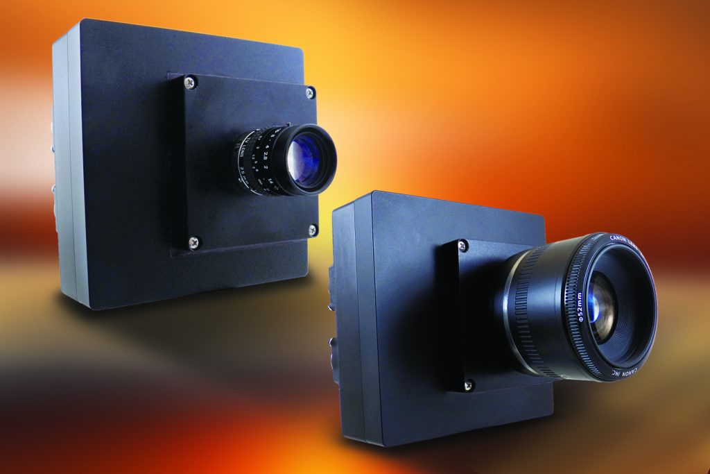
Syracuse, N.Y. – Critical Link, LLC, a leader in embedded solutions, and Canon U.S.A., Inc., a leader in digital imaging solutions, are pleased to announce availability of Evaluation Kits for two of Canon’s latest CMOS image sensors: the 120MXS, a 120MP CMOS sensor; and the 3U5MGXSBA, a 5MP global shutter sensor.
As previously announced, the companies have been collaborating on development of Sensor Evaluation Kits for Canon CMOS sensors. The kits allow developers to test sensor features and performance to ensure a fit with their application. System designers gain access to assets that accelerate development time, including complete sensor board design files. For applications that require on-board image processing, the Evaluation Kits feature an open architecture design, with the option to embed processing and software with the on-board CPU and FPGA fabric.
Evaluation Kits consist of a camera with a pre-installed Canon CMOS sensor, and include:
Accessory package for out-of-the-box operation (quick start guide, power supply, cables)
Embedded software to setup the sensor, acquire image data and communicate over USB 3.1 interface with any USB 3 compliant UI
PC-based UI application available for download to communicate with the camera
A third evaluation kit is in development for Canon’s 35MMFHDXS_A, a 19 μm, 2.76MP sensor with extreme-low-light sensitivity. Availability is projected for early 2020.
Visit Canon USA for information on new sensors and to reserve an Evaluation Kit.
Visit Critical Link for information about our embedded solutions and engineering capabilities.
About Critical Link
Syracuse, N.Y.-based Critical Link (www.criticallink.com) is an embedded systems engineering firm offering customizable system-on-modules (SOMs) and imaging platforms for industrial, medical, scientific, and defense applications. Critical Link’s end-to-end product engineering services include design, development, and production. Critical Link is a Platinum Member of the Intel (Altera) FPGA Design Solutions Network and the Intel IoT Solutions Alliance, and is ISO 9001:2015 Registered by SRI Quality System Registrar.
About Canon USA
Canon U.S.A., Inc., is a leading provider of consumer, business-to-business, and industrial digital imaging solutions to the United States and to Latin America and the Caribbean markets. With approximately $36 billion in global revenue, its parent company, Canon Inc. (NYSE:CAJ), ranks third overall in U.S. patents granted in 2018† and is one of Fortune Magazine’s World’s Most Admired Companies in 2019. Canon U.S.A. is dedicated to its Kyosei philosophy of social and environmental responsibility. To keep apprised of the latest news from Canon U.S.A., sign up for the Company’s RSS news feed by visiting www.usa.canon.com/rss and follow us on Twitter @CanonUSA.
# # #
* Available upon request.
† Based on weekly patent counts issued by United States Patent and Trademark Office.
Syracuse, N. Y. – September 18, 2019 – Critical Link, a leading provider of electronics and engineering services for industrial embedded applications, will present its latest sensor evaluation kits and board level solutions at Medical Design & Manufacturing (MD&M), Minneapolis, October 23-24, 2019. The company will premiere its new evaluation kits that feature Canon’s latest line of CMOS industrial sensors, in the main hall booth # 2416 at the Minneapolis Convention Center.
Critical Link was recently selected by Canon USA to develop evaluation platforms for cutting-edge sensors, opening up new application possibilities in the medical industry, from medical imaging to microscopy. In addition to early assessment of sensor performance, the new kits allow medical imaging system designers to accelerate development time. The kits feature an open-architecture design, with the option to embed processing and software with the on-board CPU and FPGA fabric.
“Critical Link has been enabling innovation in medical and scientific technology for more than 20 years,” notes Amber Thousand, director of marketing. “We’re excited to bring our embedded technology solutions to the Twin Cities, the largest medtech hub in the U.S.”
The company has provided embedded solutions for a wide range of medical applications including:
Lab equipment & instrumentation
Surgical equipment & instrumentation
Diagnostics
Robotic vision
Dental imaging
Critical Link will also showcase their full line of industrial performance embedded system on modules (SOMs) and embedded imaging platforms. Products on display at MD&M Minneapolis will include:
MitySOM-A10S system on module and image processing board. This family features dual core Cortex-A9 ARMs with up to 480KLE user- programmable FPGA fabric, DDR4 memory, and 12 high-speed transceiver pairs, making it an ideal solution for machine vision and scientific imaging applications. The board is available in two configurations: first as a stack- through board for use in camera designs, and second with bottom-side, rugged board-to-board connectors for integration with an industrial baseboard.
MityCAM-C50000 imaging system. It is specially designed as an evaluation platform for the CMV50000 high-speed image sensor from ams / CMOSIS. The global shutter sensor features 47.5MP resolution at 30 frames per second, mono and RGB color options, with low dark noise and high dynamic range. The innovative system provides multiple interfaces including USB3 as standard, with custom options that include CoaXPress, Camera Link, GigE, and more.
To learn more, please visit Critical Link in the main exhibit hall Booth #2416 at the Minneapolis Convention Center October 23 – 24, 2019 or visit www.criticallink.com. Free expo passes are available in advance for qualified registrants.
About Critical Link
Syracuse, N.Y.-based Critical Link (www.criticallink.com) is an embedded systems engineering firm providing system on modules (SOMs) and embedded imaging solutions for industrial performance applications. The company’s expertise in image sensor integration, system-on-chip (SoC) and field-programmable gate array (FPGA) designs, vision protocols, and signal processing has made it a leader in board-level solutions and custom designs for OEMs and embedded developers around the world. Critical Link is a Platinum Member of the Intel (Altera) FPGA Design Solutions Network and the Intel IoT Solutions Alliance, and is ISO 9001:2015 Registered by SRI Quality System Registrar.
Recognition reflects 67% three-year growth of DeWitt-based company.
SYRACUSE, N. Y. – Inc. Magazine announced yesterday that Dewitt-based Critical Link, LLC was named to its list of 5,000 fastest-growing companies in America for the second year in a row. With 2018 revenues of $12.7 million, the company achieved three-year sales growth of 67% earning a rank of No. 4454 on the prestigious list.
“Making this prestigious list a second year in a row is an honor,” said Critical Link president John Fayos. “We are proud of the growth achieved throughout our 22-year history, but are especially pleased with the tremendous increases seen in our product business these last 4 years. It is this success which has driven our overall company performance, and put us in the national spotlight.”
The Inc. 5000 list is an exclusive ranking of the nation’s fastest-growing private companies and represents the most comprehensive look at America’s entrepreneurs.
“The companies on this year’s Inc. 5000 have followed so many different paths to success,” says Inc. editor in chief James Ledbetter. “There’s no single course you can follow or investment you can take that will guarantee this kind of spectacular growth. But what they have in common is persistence and seizing opportunities.”
Critical Link employees celebrate the company’s 20th anniversary in 2017.
Critical Link is widely respected as a leader in the design and production of embedded system solutions. The DeWitt-based company joins just four others on the list from Central New York, and only 81 engineering firms nationwide. The company specializes in system-on-chip (SoC) and field-programmable gate array (FPGA) designs, sensor integration, and signal processing.
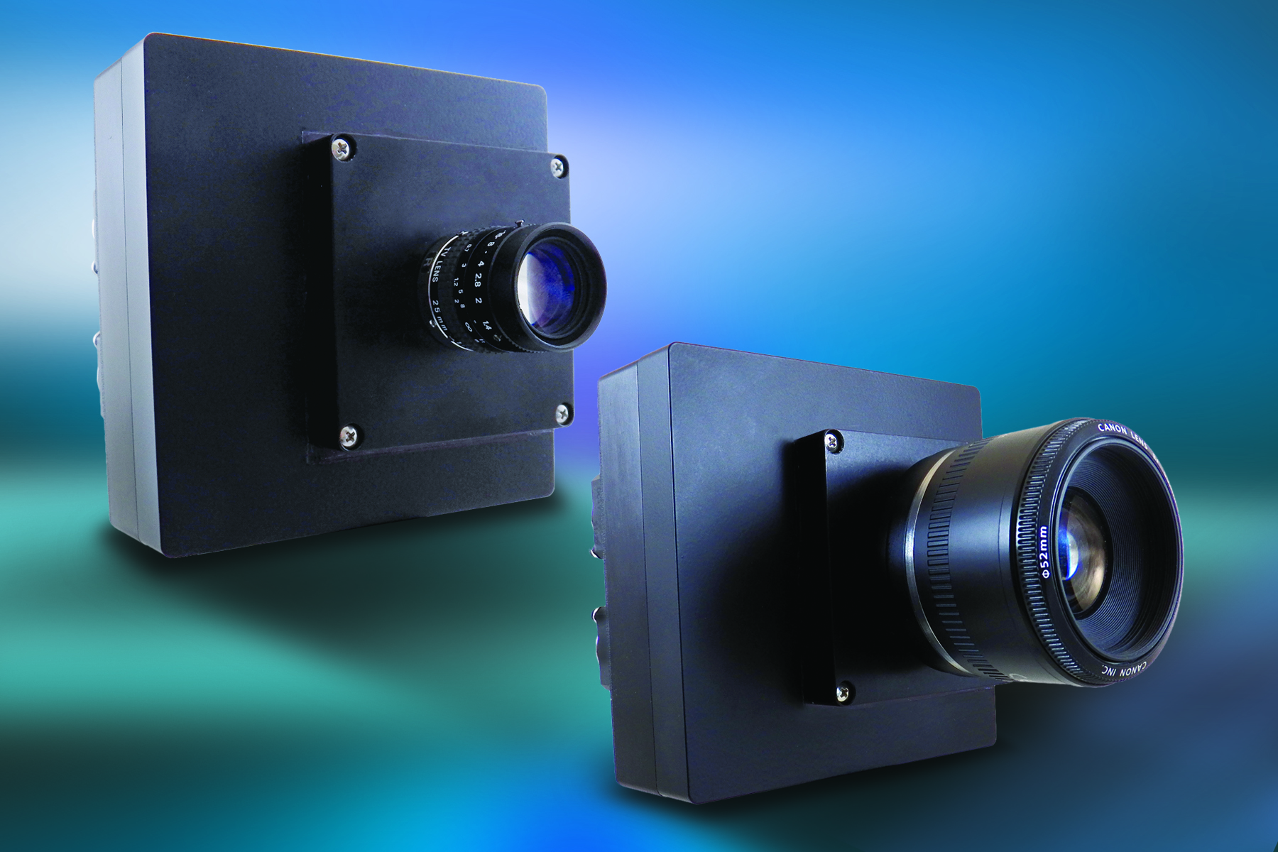
Critical Link’s Evaluation Kit for the Canon 3U5MGXSBA Sensor
Among other achievements, the company recently announced it was selected by Canon USA to develop evaluation kits for three of its industrial CMOS image sensors. These cameras are built around Critical Link’s MitySOM-A10S featuring the Intel/Altera Arria® 10 SoC processor for industrial applications.
ABOUT THE COMPANY:
Critical Link, LLC(Syracuse, NY www.criticallink.com), is an embedded system engineering firm providing system on modules (SOMs) and embedded imaging solutions for industrial performance applications. The company’s expertise in image sensor integration, system-on-chip (SoC) and field-programmable gate array (FPGA) designs, vision protocols, and signal processing has made it a leader in board-level solutions and custom designs for OEMs and embedded developers around the world.
Privately held, Critical Link is a Platinum member of the Intel FPGA Design Services Network and Intel IoT Solutions Alliance, a Platinum member of the Texas Instruments Design Network, and is ISO 9001:2015 Registered by SRI Quality System Registrar.
MELVILLE, N.Y., JULY 25, 2019— Critical Link, LLC, a leader in embedded solutions is pleased to share thatCanon U.S.A., Inc., a leader in digital imaging solutions announced the company has selected Critical Link, to develop new Evaluation Kits for three of Canon’s CMOS image sensors: the 120MXS, a high resolution 120MP sensor; the 35MMFHDXS_A, a high sensitivity 19μm pixel size, 2.76MP sensor; and the 3U5MGXSBA, a 5MP global shutter sensor.
Currently in development by the Critical Link engineering team, these kits will allow developers to test the features and performance of each of the Canon CMOS sensors to ensure a fit with their application. In addition to early assessment of sensor performance, image system designers will gain access to assets that accelerate development time including complete sensor board design files. For applications that require on-board image processing, the evaluation kits feature an open architecture design, with the option to embed processing and software with the on-board CPU and FPGA fabric.
“Critical Link is honored to be selected by Canon to develop three new Evaluation Kits,” said Omar Rahim, VP of Imaging Product Sales at Critical Link. “We believe the performance and pixel design of Canon’s CMOS sensors will appeal to OEMs and end users, and that Evaluation Kits will help customers accelerate innovation in industrial vision.”
“We are excited and proud to select Critical Link to help introduce these CMOS Sensor Evaluation Kits into the marketplace. These will allow customers to better test our sensor capabilities and accelerate the design process of their imaging systems,” said Kazuto Ogawa, president and chief operating officer, Canon U.S.A., Inc.
Each Evaluation Kit consists of a camera with a pre-installed Canon CMOS sensor, and will include:
Accessory package for out-of-the-box operation (quick start guide, power supply, compact tripod, cables)
Embedded software to setup the sensor, acquire image data and communicate over USB 3.1 interface with any USB 3 compliant UI
PC-based UI application available for download to communicate with the camera
Sensor board design files and source code*
VHDL code for the FPGA*
Visit Canon U.S.A. CMOS sensors for updated information and to reserve an Evaluation Kit. The kits will be available later in the year.
About Critical Link Syracuse, N.Y.-based Critical Link (https://www.criticallink.com/) is an embedded systems engineering firm offering customizable system-on-modules (SOMs) and imaging platforms for industrial, medical, scientific, and defense applications. Critical Link’s end-to-end product engineering services include design, development, and production. Critical Link is a Platinum Member of the Intel (Altera) FPGA Design Solutions Network and the Intel IoT Solutions Alliance, and is ISO 9001:2015 Registered by SRI Quality System Registrar.
About Canon U.S.A., Inc. Canon U.S.A., Inc., is a leading provider of consumer, business-to-business, and industrial digital imaging solutions to the United States and to Latin America and the Caribbean markets. With approximately $36 billion in global revenue, its parent company, Canon Inc. (NYSE:CAJ), ranks third overall in U.S. patents granted in 2018† and is one of Fortune Magazine’s World’s Most Admired Companies in 2019. Canon U.S.A. is dedicated to its Kyosei philosophy of social and environmental responsibility. To keep apprised of the latest news from Canon U.S.A., sign up for the Company’s RSS news feed by visiting www.usa.canon.com/rss and follow us on Twitter @CanonUSA.
###
†Based on weekly patent counts issued by United States Patent and Trademark Office.
Embedded Vision is a hot topic in many industrial spaces. The integration of data processing on board a camera without the need for a back-end PC, server, or other costly system has system developers — in industries from factory test and measurement to agriculture, and from autonomous driving to medical diagnostics — looking for ways to move processing closer to the sensor. Doing so can lead to lower recurring costs, faster performance, and an optimized footprint (that is, low size, weight, power, and cost — or low SWaP-C), and systems that are more agile and able to evolve with changing requirements. This means innovation and growth in industrial markets across the world will be heavily affected by advancements in embedded vision.
Cities, factories, and transportation systems are implementing vision-based technologies to improve efficiency, performance, cost, reliability, and safety.
Moving from a traditional PC- or server-supported vision system to an embedded platform does not happen overnight, and it requires an investment in upfront engineering and development. There are several key factors developers should consider early on when planning to transition from a traditional vision system to a new embedded vision design. Evaluating these factors ahead of time will help ensure a product that meets current system performance requirements, while allowing for application growth and long-term design stability.
Processing technology
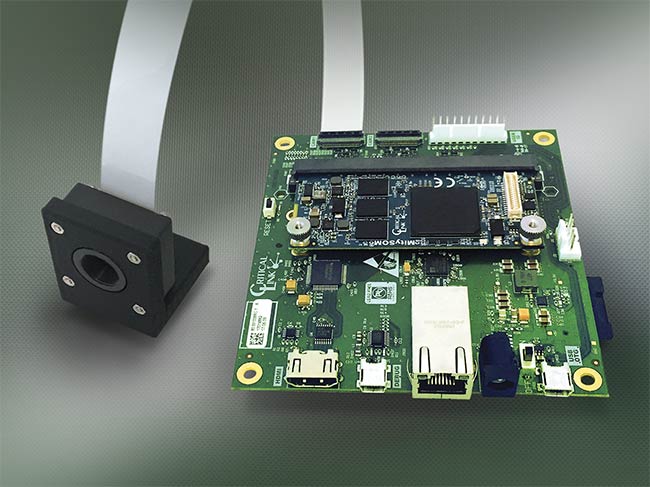
One of the first questions developers may ask is on which processing technology they should base their design. The answer is becoming increasingly complex because processing performance and speed have escalated so rapidly that developers are able to acquire and process images faster, even when implementing higher-resolution sensors (Figure 1).
Figure 1. An embedded vision board integrated with a camera module.
CPUs (central processing units), GPUs (graphics processing units), and FPGAs (field-programmable gate arrays) each offer distinct advantages for embedded vision systems. Furthermore, the growing number of chip and board manufacturers in the marketplace makes the decision not only about the processing technology, but also about the supply chain, quality, support, and longevity of the product being developed.
CPUs
CPUs are easy to program and compile, and they offer versatility in that they can execute a wide range of functionality. Typically, they also include a host of analog and digital peripherals. CPUs perform processing operations in sequence. For vision applications, one operation must run on an entire image before the next operation can begin. Multicore CPUs allow for some level of parallel operation (albeit far less than GPUs or FPGAs), increasing performance but not affecting programmer friendliness.
Given their sequential nature, CPUs remain the best architecture for applications in which algorithms such as pattern matching or optical-character recognition will be used. This type of processing analyzes the entire image and compares it to a master data set. CPUs are most efficient here because of their extremely fast clock speeds and direct access to typically large amounts of memory.
GPUs
GPUs are similar to multicore CPUs in that GPUs are made of a series of logic cores, each of which is capable of performing operations sequentially. GPUs are composed of many more and smaller logic cores, however. So although multicore CPUs — most often with two to four cores — can perform a small amount of parallel processing, GPUs can handle orders of magnitude more, with up to multihundreds of logic cores.
GPUs have grown in popularity in the embedded vision space, in part because they are well suited for applications where simple operations can be performed in parallel and continuously on large data sets. As an example, GPUs offer a tremendous benefit in artificial intelligence (AI) training applications, where the ability to process massive data sets in relatively short amounts of time is essential. When it comes to AI inferencing, however, FPGAs tend to have the best performance, followed by GPUs.
GPUs excel at functions such as video post-processing, and they offer optimized efficiency for floating-point computations and matrix math. The trade-off is that they consume high amounts power, which can pose a challenge in embedded vision systems where portability or low SWaP-C matters.
GPUs tend to be best for consumer designs or products that will go through frequent design upgrades, rather than for industrial, medical, or other long-lifespan products. This is because although the performance lifespan of a GPU can easily extend to a decade, most GPU devices remain on the market for only 18 to 36 months, after which they are considered obsolete and are replaced by next-generation devices.
FPGAs
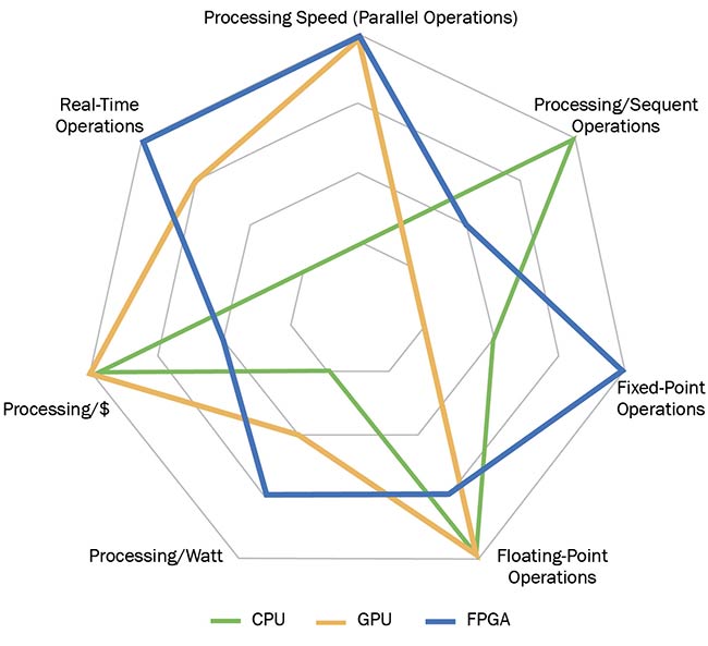
At the highest levels of processing, FPGAs provide the greatest advantages in speed and flexibility. Given their highly efficient parallel-processing capability, FPGAs are more suitable than CPUs or GPUs for real-time processing and multiple-interface applications. They are reprogrammable, with flexibility for design changes and new functionality that cannot be achieved with any other architecture (Figure 2).
Figure 2. A performance comparison between a CPU, GPU, and an FPGA, noting key image-processing characteristics.
In terms of energy efficiency — an important consideration in embedded systems design — FPGAs are superior to both CPUs and GPUs. This is especially true for performing algorithms based on logic and fixed-precision computations. The two biggest names in FPGAs have supported device families for a decade or more. Going forward, this means developers of industrial, medical, and other long-lifespan applications can depend on device availability and on access to product support for the life of a device’s design.
Traditionally, FPGAs have been the most difficult to program, requiring developers to have special skills in hardware description languages (HDLs), such as VHDL or Verilog. Long cycles to compile a design are also necessary. However, many tools are available today to make programming an FPGA faster and easier, even without expertise in HDLs. Two examples are OpenCL and high-level synthesis (HLS), which enable targeting C/C++ code to the FPGA. Learning to use these tools can take time; fortunately, many manufacturers offer software development kits that make it easier to get started. Developers can then use such tools to leverage other benefits as well, including the ability to accelerate application code, reduce power usage, and drastically reduce compile times.
For an even easier way to program FPGAs, graphical programming tool kits now enable image-processing functions to be implemented using visual-programming pipelines. A growing number of suppliers are launching tools in which image-processing functions — from pixel correction and color processing to trigger functionality and segmentation — can be graphically pipelined and then implemented into the FPGA. These are not yet universal solutions, but expect to see rapid expansion in this area in years to come.
Alternatively, FPGAs allow for off-the-shelf intellectual property (IP) blocks to be integrated into the fabric, bypassing lengthy development cycles and giving streamlined functionality. Many embedded board and camera vendors provide IP blocks already embedded in their solutions for image preprocessing functions such as compression, white balancing, debayering, and noise reduction. Beyond these basics, IP blocks are available from a range of vendors for application-specific processing tasks including object measurement and tracking, stereo vision, motion detection, and many others. IP blocks can also be used to implement a variety of interfaces.
Heterogeneous architecture
In many cases, developers will include more than one processing technology in their design, most often combining an FPGA with either a CPU or GPU. This means the two devices share the processing load, each one taking on the tasks it is best suited to handle.
For example, in a heterogeneous system-on-chip (SoC) architecture where a CPU and FPGA are both present, developers can optimize their design for the strengths of each device. Depending on the interface, the CPU may be best for image acquisition, and then the developer may transfer the image to the FPGA for preprocessing tasks such as noise reduction or debayering. Images can then be processed in parallel in the FPGA or sent back to the CPU for iterative functions. Even with these transfers, such a pipeline can be more efficient than a single- processing architecture.
There is no universally correct answer to the complex question of which processing architecture to choose. Choosing the right technology is a function of multiple factors and is highly dependent on not only the technology but the support system around it.
Design support
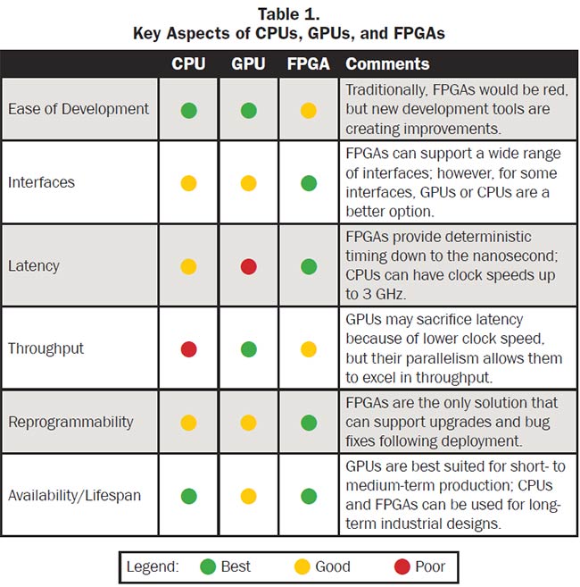
Executing a new embedded vision product design typically requires factory support for issues such as sensor integration, software and image processing, interface development, or all of the above. Questions come up throughout the design process that can be answered by an array of sources: data sheets, community forums, application engineering support, and direct factory interaction. Depending on a company’s size and reach, some resources may be more accessible than others. It’s important to consider how support will be delivered for the products you’ve selected (Table 1).
Table 1. Key aspects of CPUs, GPUs, and FPGAs
If the in-house team is knowledgeable and has extensive experience in imaging design, access to thorough documentation or community forums may be enough. Previous experience with a sensor, interface spec, and processing technology can mean major efforts will be focused on the application software and processing functions — the IP — that your team is developing.
Although the performance lifespan of a GPU can easily extend to a decade, most GPU devices remain on the market for only 18 to 36 months.
If the technologies being integrated into the design are not familiar to the team, however, it’s important to understand whether access to application engineering support will be available from the manufacturer or its channel partners. As the pressure to operate more efficiently has grown for major manufacturers, many have pulled back on direct support to customers. In some cases, the manufacturers’ distribution partners have stepped in to provide design support through their local branches.
Alternatively, off-the-shelf components can be selected or an outside engineering services provider can be engaged to help with the design. Either option can stream- line the development schedule and allow the team to dedicate its focus on generating value-added IP. Working with an engineering services provider that is familiar with the technologies and brands selected means many design challenges can be cleared faster, sometimes leveraging existing building blocks. Or, if the upfront investment in cost or schedule is not feasible, off-the-shelf development kits can provide a platform for low-cost, rapid prototyping.
Successful transitions
A growing shortage of hardware engineers means fewer companies have the manpower to develop new production-suitable hardware from the ground up. Open-source platforms that help people learn programming have offered relief, and for many applications, these solutions can be viable for production. However, when it comes to industrial or medical-grade systems, a transition path is needed to ensure long-term production and design stability. The question then becomes: What can be done early on to ensure the prototype is suitable for production, or to ensure that a viable transition plan exists?
This question was partly addressed in the discussion of processing technologies above, showing that certain architectures are designed for longer availability than others. The same is true for image sensors and cameras, as well as for all the other components designed into a new product. When selecting any of these components for a final design, it is very important for the system designer to be aware of availability projections. Working with an off-the-shelf board can often alleviate problems of availability, since the board supplier manages the supply chain and deals with obsolescence issues. Developers should look for a reputable supplier that publishes product change notifications (PCNs), that does not change part numbers frequently, and that will provide patches and engineering support in the event that a change is necessary. These are healthy signs that the supplier maintains its board designs over time.
Low-volume, short-term production, or designs that will go through frequent changes will probably not be affected by the above factors. However, if the product is intended for medium- to high-volume production and/or long-term availability, the design team should factor this in up front when evaluating which processing platform to use.
Flexibility for the future
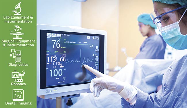
Finally, developers should know how much flexibility or additional headroom is needed to accommodate future application changes, feature growth, or advanced processing. Some designs remain relatively fixed for the life of the product, with little need to integrate new features or capabilities. Others, however, are used in industries that are constantly evolving (Figure 3). The inability to implement new processing techniques or application software upgrades could hurt sales and cripple return on investment. This is true in areas such as manufacturing and warehousing, smart cities and infrastructure, energy and utilities, and transportation. The wave of embedded vision integration is still far from cresting in these areas, and developers who allow room for their design to grow as technology advances will be better positioned for long-term success.
Figure 3. Embedded imaging systems have already made their way into medical and scientific applications, and they are gaining even more momentum as the health care industry drives toward higher standards and leaner processes.
Meet the authors
Dave Rice is co-founder of Critical Link and vice president of its engineering division. He has led the company’s technology development efforts for more than 20 years. Rice has a bachelor’s degree in electrical engineering from Penn State University; email: david .rice@criticallink.com.
Amber Thousand is the director of marketing at Critical Link, working with engineering on product development. She has a bachelor’s degree from Elon University and a master’s in business administration from the University of Phoenix; email: athousand@criticallink.com.
Company will present two technical sessions on embedded imaging solutions at the Embedded Technologies Expo Conference, McEnery Convention Center, San Jose, California, while showcasing its award-winning systems, boards, and platforms in Booth #1835, June 25-27, 2019.
Critical Link’s MitySOM-A10S & MityCAM-C50000
Syracuse, N. Y. – Critical Link, a leading provider of electronics and engineering services for industrial embedded applications, will present two technical sessions and showcase its latest board-level embedded imaging solutions at the inaugural Embedded Technologies Expo & Conference (ETC), McEnery Convention Center, San Jose, California, from June 25-27, 2019. The expo will be co-located with the Sensors Expo & Conference, the largest of its kind in North America.
“We’re excited to be part of the first Embedded Technologies Expo & Conference,” said Amber Thousand, director of marketing. “The co-location with the popular Sensors Expo represents a sweet spot for Critical Link’s embedded imaging solutions.”
Critical Link’s technical presentations are part of the “Vision & Imaging for Industrial Applications” track of the conference program. On Thursday, June 27 at 10:00 a.m, co-founder and vice president of imaging applications, Omar Rahim, will present “Using Linux with FPGA Co-Processing for Real-Time Embedded Vision.” Following at 11:25 a.m., Dave Rice, co-founder and technical director, will give a talk entitled “Optimizing Industrial Imaging Development.” Conference registration is required for both sessions which will take place in room 203A.
Critical Link’s System on Modules (SOMs) and embedded imaging platforms are designed for next-generation performance in a variety of scientific, industrial, medical, and defense applications to ensure a faster time to market, lower development costs, and long-term availability. Products on display at ETC will include:
MityCAM-C50000imaging system. Specially designed as an evaluation platform for the CMV50000 high-speed image sensor from ams / CMOSIS. The global shutter sensor features 47.5MP resolution at 30 frames per second, mono and RGB color options, with low dark noise and high dynamic range. The innovative system provides multiple interfaces including USB3 as standard, with custom options that include CoaXPress, Camera Link, GigE, and more.
MitySOM-A10S system on module (SOM) and image processing board. This family features dual core Cortex-A9 ARMs with up to 480KLE user- programmable FPGA fabric, DDR4 memory, and 12 high-speed transceiver pairs, making it an ideal solution for machine vision and scientific imaging applications. The board is available in two configurations: first as a stack- through board for use in camera designs, and second with bottom-side, rugged board-to-board connectors for integration with an industrial baseboard.
The MityCAM-C50000 and the MitySOM-A10S are readily available from Critical Link and select partners. To see a demonstration of these remarkable new embedded imaging solutions, please visit Booth #1835 at the Embedded Technologies Expo & Conference, McEnery Convention Center, San Jose, California, June 25-27, 2019. For more information, please go to www.criticallink.com or email us at info@criticallink.com.
About Critical Link Syracuse, N.Y.-based Critical Link (www.criticallink.com) is an embedded systems engineering firm offering customizable system-on-modules (SOMs) and imaging platforms for industrial, medical, scientific, and defense applications. Critical Link’s end-to-end product engineering services include design, development, and production. Critical Link is a premier Partner in the Imaginghub by Basler, a Platinum Member of the Intel (Altera) FPGA Design Solutions Network and the Intel IoT Solutions Alliance, and is ISO 9001:2015 Registered by SRI Quality System Registrar.
Critical Link’s Director of Marketing Recognized at Crystal Ball Ceremony
SYRACUSE, N. Y. – Critical Linkis
pleased to recognize its Marketing Director, Amber Thousand, with a CNY Sales
& Marketing Excellence Award. This award honors individuals with
demonstrated success in the sales and marketing profession and was presented at
the 43rd Annual Crystal Ball hosted by CNY Sales & Marketing
Executives.
Critical
Link hired Amber in 2013 to establish a dedicated marketing effort. Since that
time, she has become a key contributor to Critical Link’s
business strategy which has propelled the company’s revenue more than 73% in
the last three years.
“One
of Amber’s many strengths is her ability to see gaps in the company and fill
them,” said John Fayos, Critical Link co-founder and president. “She isn’t
afraid to step-up and implement change and there are few areas she hasn’t
improved.”
Among
those improvements, Amber helped redefine Critical Link’s value proposition and
go-to-market approach, implemented a new sales model, and established new
processes to shift Critical Link from a services-based company, to a
product-based one. Her leadership has helped the
company grow, including more than tripling the number of system on modules sold
each year.
“Amber helps us
make our own luck,” said Tom Catalino, co-founder and vice president of sales.
“And as a result, we’re reaching more customers than ever before.”
Without a team or
large budget to execute initiatives, Amber has strengthened and leveraged
relationships to expand Critical Link’s reach. This has included distributors,
technology partners, manufacturers, media, rep firms, and more.
“It’s
an honor to be recognized among such a great group of professionals,” said Thousand.
“I am thrilled every day for my role at Critical Link. But the success we have
had, and will continue to have in the years to come, is made possible because
of the strength and contributions of the entire team.”
Amber accepted her
award at the 43rd Annual Crystal
Ball hosted by CNY Sales & Marketing Executives at the Marriott Syracuse
Downtown on April 30th. Amber was one of 12 professionals bestowed
with this award. Visit www.cnysme.org for a full list of winners.
Central New York Sales & Marketing Executives (CNYSME) was founded in 1935 and is the area’s recognized voice of the sales and marketing profession, the only organization focused exclusively on the needs of the sales and marketing professionals.
About Critical Link
Founded
in 1997, Critical Link designs and manufactures board level processing cards
(called System on Modules) and embedded imaging platforms for industrial
electronic applications worldwide. The company delivers advanced technology
solutions for customers in manufacturing, energy and utilities, defense,
medical, laboratory science, transportation, and many others.
The company is owned and operated by its original co-founders and employs 42 people at its facility in Dewitt. And we’re hiring! To learn more, visit www.criticallink.com and follow us on LinkedIn.
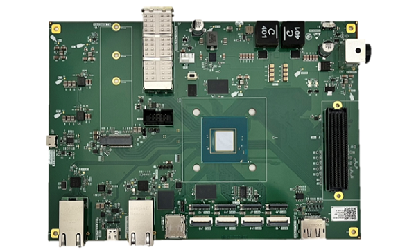 The MitySBC-A5E single-board computer was developed as part of the Agilex 5 SoC FPGA Early Access Program and will be the first to market. The MitySBC-A5E features a 32mm x 32mm Agilex 5 SoC FPGA E-Series with 656K LE FPGA fabric, dual-core Cortex-A55, dual-core Cortex-A76, PCIe 3.0, and 24 transceivers up to 17Gbps. The board includes 8GB LPDDR4 for the HPS, 8GB LPDDR4 for the FPGA, 64GB eMMC, microSD, and QSPI NOR for configuration. A rich set of interfaces, including 8 MIPI x4 lanes, 2.5G Ethernet, FMC, USB-C & USB 2, among others, make this a powerful solution for embedded product development teams working on next-generation industrial performance applications.
 Following the introduction of the single board computer, Critical Link is bringing the MitySOM®-A5E family of system-on-modules to market later this year. The MitySOM-A5E family will offer a wide range of FPGA densities, memory configurations, optional transceivers, and temperature ranges all in a compact 51mm x 71mm (2.0” x 2.8”) form factor to fit most applications. These modules are designed for long-term availability and support, meaning customers can confidently design them into long lifespan products in the test & measurement, medical/scientific, defense, and energy/utilities industries.