Visit Critical Link booth #1019 at the Del Mar Electronic & Manufacturing Show and earn professional development hours at our Embedded Design Challenges seminar. Space is limited, register today!
Syracuse, N.Y. – April 30, 2024 – Critical Link, LLC, a leading US-based manufacturer of FPGA, DSP, and CPU-based System on Modules, is pleased to announce new embedded solutions around the AgilexTM 5 SoC FPGA E-Series from Altera®. Critical Link is developing two product families around the Agilex 5 SoC FPGA E-Series: a single board computer and a system on module (SOM) family.
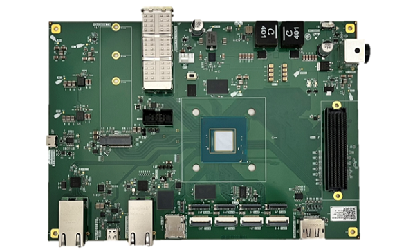 The MitySBC-A5E single-board computer was developed as part of the Agilex 5 SoC FPGA Early Access Program and will be the first to market. The MitySBC-A5E features a 32mm x 32mm Agilex 5 SoC FPGA E-Series with 656K LE FPGA fabric, dual-core Cortex-A55, dual-core Cortex-A76, PCIe 3.0, and 24 transceivers up to 17Gbps. The board includes 8GB LPDDR4 for the HPS, 8GB LPDDR4 for the FPGA, 64GB eMMC, microSD, and QSPI NOR for configuration. A rich set of interfaces, including 8 MIPI x4 lanes, 2.5G Ethernet, FMC, USB-C & USB 2, among others, make this a powerful solution for embedded product development teams working on next-generation industrial performance applications.
The MitySBC-A5E will be available as a development kit as well as a production-suitable single-board computer for customers interested in achieving first-to-market advantages with the high-performance, low-power Agilex 5 SoC FPGA. The product datasheet and other documentation are available today, and customers will benefit from Critical Link’s engineering and application support for the life of their product.
“Critical Link has been partnering with Altera and Intel for more than 10 years, helping customers reach the market fast with next-generation products based on the latest FPGA technology,” says Tom Catalino, Vice President and Founder of Critical Link, LLC. “We are excited to lead the next wave of FPGA-based designs and bring the Agilex 5 SoC FPGA power and performance advantages to our customers.”
 Following the introduction of the single board computer, Critical Link is bringing the MitySOM®-A5E family of system-on-modules to market later this year. The MitySOM-A5E family will offer a wide range of FPGA densities, memory configurations, optional transceivers, and temperature ranges all in a compact 51mm x 71mm (2.0” x 2.8”) form factor to fit most applications. These modules are designed for long-term availability and support, meaning customers can confidently design them into long lifespan products in the test & measurement, medical/scientific, defense, and energy/utilities industries.
Prototypes for the MitySBC-A5E will be available in Q2 2024, with production in early 2025. System on Module prototypes are expected later this year with production to start in 2025.
For more details on the MitySBC-A5E Single Board Computer, visit: https://www.criticallink.com/product/mitysbc-a5e-single-board-computer/.
For more details on the MitySOM-A5E System on Module family, visit: https://www.criticallink.com/product/mitysom-a5e/.
ABOUT THE COMPANY:
Critical Link, LLC (Syracuse, NY www.criticallink.com), founded in 1997, develops system on modules (SOMs) for electronic applications. Our MitySOM® and MityDSP® families incorporate the latest FPGA, DSP, and CPU technologies, and are designed for long product lifespan and performance in the field. We supply OEMs in a wide range of industries including manufacturing, medical, scientific, defense, and energy/utilities. We ship worldwide and are franchised with many of the top electronics distributors.
Critical Link, LLC, is privately held and is ISO 9001:2015 Registered by SRI Quality System Registrar. Critical Link is a Gold-level member of the Intel® Partner Alliance.
*Altera Agilex 5 FPGA D-series (A5D031, mid-speed grade) vs. AMD/Xilinx Versal (VM1102, -3HS speed grade) at 90% utilization, 600-Mhz, using vendors power estimator calculators.
Altera, the Altera logo, and other Altera marks are trademarks of Altera or its subsidiaries.
“The customers who come to Senseeker are also often looking for other specialist electronics, and that’s where Critical Link fits in. They have a reputation for quality, and a long track record of working with complex applications. We wanted them to be part of our ecosystem,”
— Ross Bannatyne, Senseeker Director of Business Development
When Senseeker approached Critical Link about partnering, Critical Link was more than interested. Senseeker specializes in infrared image sensing products and services. Their state-of-the-art digital imaging sensors and readout integrated circuits for hybrid infrared image sensing arrays are used in cutting-edge security, military, and machine vision applications – the types of application where Critical Link technology is often embedded.
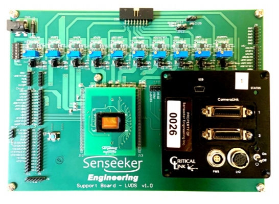
For Critical Link, working with Senseeker would be a partnership with a twist. Critical Link’s traditional partnerships have been formed with technology providers whose hardware and software are integral to the company’s System on Modules (SOMs). With Senseeker, Critical Link would be providing a key component of the Evaluation Kits for their Oxygen® RD0092, an off-the-shelf digital readout IC (DROIC) and Magnesium® MIL RP0092 digital pixel readout IC (DPROIC).
Senseeker’s Oxygen® RD0092 is the world’s first 8 μm pitch dual-band DROIC, providing infrared image system developers access to state-of-the-art technology without incurring the cost and risk associated with ground-up, custom designs. Used in defense and security applications such as infrared search and track and situation awareness, the Oxygen RD0092 is available to developers off-the-shelf in wafer form and is supported with an Evaluation Kit that expedites the infrared image sensing development cycle.
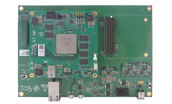
The Evaluation Kit includes an image acquisition support board from Critical Link, an engineering firm that develops embedded solutions for a wide range of electronic applications. The Critical Link support board captures high-speed digital data acquired from the Senseeker readout IC, converts it for use, and transmits it for display to a host PC containing a commercial frame grabber card. The image acquisition support board that makes up part of the Evaluation Kit is based on Critical Link’s MitySOM-5CSx, a highly-configurable small form-factor System on Module (SOM). The MitySOM-5CSx is designed for high-throughput applications requiring single or dual hard-core Cortex-A9 applications processors tightly integrated with FPGA fabric. The MitySOM-5CSx combines the Altera Cyclone V System on Chip (SoC), memory subsystems and onboard power supplies, including two Camera Link ports. The MitySOM-5CSx provides a complete and flexible CPU and FPGA infrastructure for highly-integrated embedded systems.
The image acquisition support board is designed to be supplied by an external 5V supply, and provides adjustable detector bias voltages. It also includes connections for an optional external clock input, as well as numerous digital and analog test points. The board supports both room temperature (uncooled) and cryogenic (cooled) evaluation.
Ross Bannatyne is Senseeker’s Director of Business Development. “The customers who come to Senseeker are also often looking for other specialist electronics, and that’s where Critical Link fits in. They have a reputation for quality, and a long track record of working with complex applications. We wanted them to be part of our ecosystem,” Bannatyne says. Senseeker is currently transitioning from a pure custom-design producer to a company that offers both custom design and custom-off-the-shelf products. “When we first began talking with Critical Link, we found that, many years ago, they’d also made this type of transition, so it’s an especially good match. Critical Link just gets us.”
“We’re excited to be partnering with Senseeker,” says Tom Catalino, co-Founder and Vice President of Critical Link. “Early on in our discussions, we realized that we not only shared a passion for electronics, but that our core values are in sync. We’re both committed to excellence, and to making it possible for our clients to accelerate product development without having to sacrifice on quality, cost, or the ability to easily make the customizations that that make their products unique.”
About Critical Link
Syracuse, NY-based Critical Link (www.criticallink.com) is an embedded systems engineering firm, offering a broad range of customizable SOMs and cameras for industrial performance applications. Critical Link’s end-to-end product engineering offerings include design, development, and production services. The company’s expertise in image sensor integration, system-on-chip (SoC) and field-programmable gate array (FPGA) designs, vision protocols, and signal processing has made it a leader in board-level solutions and custom designs for OEMs and embedded developers around the world. Privately held, Critical Link is a Platinum member of the Intel FPGA Design Services Network and Intel IoT Solutions Alliance, a Platinum member of the Texas Instruments Design Network, and is ISO 9001:2015 Registered by SRI Quality System Registrar.
Syracuse, N.Y. – The JESD204B serial interface has become the interface standard of choice for high-speed analog-to-digital and digital-to-analog converters (ADCs and DACs). Intel® FPGAs and Intel® SOC FPGAs are well suited to interface to these converters using this interface and Arrow Electronics™ has developed four JESD204B reference solutions using high-speed analog RF transceivers and converter modules based on Analog Devices RF transceivers, ADCs, and DACs. These solutions employ third party carrier board platforms from Critical Link supporting production-ready Systems on Modules (SOMs) based on Intel® Arria® 10 SOC FPGAs.
The hardware for each of these platforms includes:
Example reference designs for the platforms include:
Each reference platform also includes a unique Quick Start Guide and complete source code for an example design. All documentation is now freely available on GitHub.
The four Arrow Electronics reference platforms are:
The ADRV9371 Platform: The ADRV9371 Platform is a complete development platform for applications that require high-performance radios capable of operating over a wideband frequency range. This platform is based on the Analog Devices AD9371 dual RF transceiver, which has a tunable range of 300 MHz to 6000 MHz. The ADRV9371 FMC converter evaluation board connects to the Intel Arria 10 SoC FPGA using the JESD204B serial interface over an FMC connector at lane rates as high as 6.144 Gbps.
The ADRV9375 Platform: Similar to the ADRV9371 Platform, the ADRV9375 Platform connects an Intel Arria 10 SoC FPGA to an ADRV9375 evaluation board through an FMC connector using a JESD204B serial interface operating at lane rates as high as 6.144 Gbps. The Analog Devices ADRV9375 evaluation board is based on the Analog Devices AD9375 dual RF transceiver, which is similar to the Analog Devices AD9371 dual RF transceiver, but the AD9375 dual RF transceiver adds an on-chip digital pre-distortion (DPD) algorithm block.
The AD-FMCDAQ2 Platform: This platform connects an Intel Arria® 10 SoC FPGA to an AD-FMCDAQ2 evaluation board over an FMC connector using the JESD204B serial interface operating at lane rates as high as 6.144 Gbps. The AD-FMCDAQ2 evaluation board incorporates an Analog Devices AD9144 high-speed DAC and an Analog Devices AD9680 high-speed ADC.
The ADRV9371, ADRV9375, and AD-FMCDAQ2 reference platforms are ideal for developing a wide range of RF applications including:
The ADRV9009 Platform: This platform connects an Intel Arria® 10 SoC FPGA to an Analog Devices ADRV9009 evaluation board over an FMC connector using the JESD204B serial interface operating at lane rates as high as 12.288 Gbps. The Analog Devices’ ADRV9009 is a wide bandwidth, high performance RF integrated transceiver with dual transmitters; dual receivers; and a dual-input, shared-observation receiver. This platform is ideal for developing a wide range of RF applications including:
Loaner kits are available from Arrow Electronics for customers to evaluate these solutions. Please contact your local Arrow rep for more information.
Article provided courtesy of Intel, original post: https://blogs.intel.com/psg/arrow-electronics-develops-a-series-of-four-complete-rf-reference-platforms-based-on-the-intel-arria-10-soc-fpga-and-analog-devices-high-speed-rf-transceivers-adcs-and-dacs/
© Intel Corporation. Intel, the Intel logo, and other Intel marks are trademarks of Intel Corporation or its subsidiaries. Other names and brands may be claimed as the property of others.
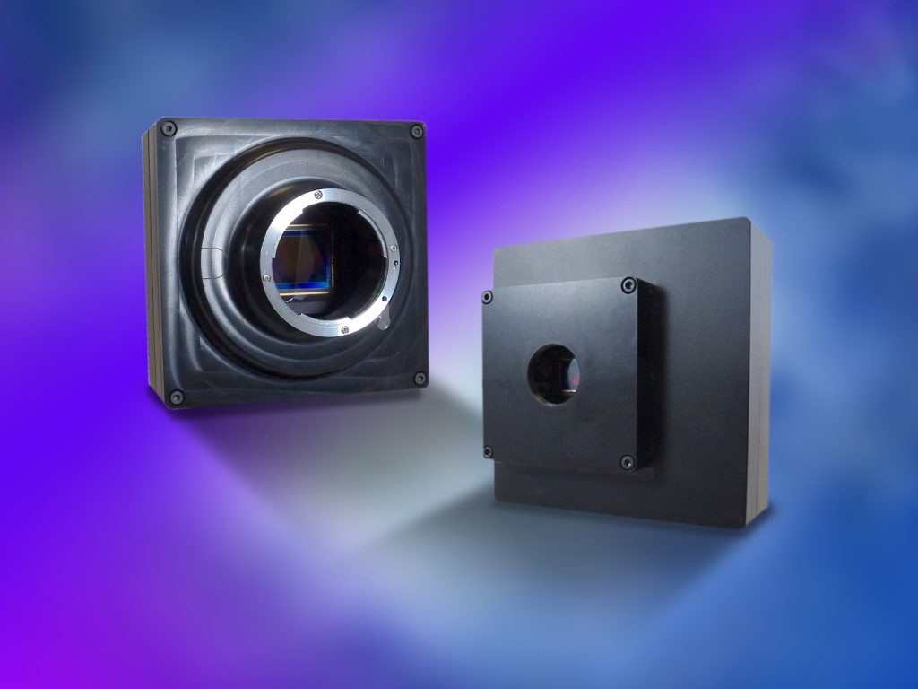
 Syracuse, N.Y. – Critical Link, LLC, a leader in embedded solutions, and Canon U.S.A., Inc., a leader in digital imaging solutions, are pleased to announce availability of Evaluation Kits for two of Canon’s latest CMOS image sensors: the 120MXS, a 120MP CMOS sensor; and the 3U5MGXSBA, a 5MP global shutter sensor.
As previously announced, the companies have been collaborating on development of Sensor Evaluation Kits for Canon CMOS sensors. The kits allow developers to test sensor features and performance to ensure a fit with their application. System designers gain access to assets that accelerate development time, including complete sensor board design files. For applications that require on-board image processing, the Evaluation Kits feature an open architecture design, with the option to embed processing and software with the on-board CPU and FPGA fabric.
Evaluation Kits consist of a camera with a pre-installed Canon CMOS sensor, and include:
Evaluation kits for the 3U5MGXSBA and the 120MXS are expected to begin shipping in November. Orders can be placed through Canon’s website, or with an authorized distributor.
A third evaluation kit is in development for Canon’s 35MMFHDXS_A, a 19 μm, 2.76MP sensor with extreme-low-light sensitivity. Availability is projected for early 2020.
Visit Canon USA for information on new sensors and to reserve an Evaluation Kit.
Visit Critical Link for information about our embedded solutions and engineering capabilities.
About Critical Link
Syracuse, N.Y.-based Critical Link (www.criticallink.com) is an embedded systems engineering firm offering customizable system-on-modules (SOMs) and imaging platforms for industrial, medical, scientific, and defense applications. Critical Link’s end-to-end product engineering services include design, development, and production. Critical Link is a Platinum Member of the Intel (Altera) FPGA Design Solutions Network and the Intel IoT Solutions Alliance, and is ISO 9001:2015 Registered by SRI Quality System Registrar.
About Canon USA
Canon U.S.A., Inc., is a leading provider of consumer, business-to-business, and industrial digital imaging solutions to the United States and to Latin America and the Caribbean markets. With approximately $36 billion in global revenue, its parent company, Canon Inc. (NYSE:CAJ), ranks third overall in U.S. patents granted in 2018† and is one of Fortune Magazine’s World’s Most Admired Companies in 2019. Canon U.S.A. is dedicated to its Kyosei philosophy of social and environmental responsibility. To keep apprised of the latest news from Canon U.S.A., sign up for the Company’s RSS news feed by visiting www.usa.canon.com/rss and follow us on Twitter @CanonUSA.
# # #
* Available upon request.
† Based on weekly patent counts issued by United States Patent and Trademark Office.