Principal Engineer at Critical Link to be honored at April 8 Banquet
Mike Williamson accepts 2019 Technologist of the Year Award from TACNY President.
SYRACUSE, N. Y. – Critical Link, LLCis pleased to announce Michael Williamson’s
selection as the 2019 Technologist of the Year by the Technology Alliance of
Central New York (TACNY). This award recognizes a resident of Central New York
who has made recent outstanding contributions to advances and improvements in a
STEM field, not limited to engineering.
“Impressive
technologies depend on having impressive technologists, so TACNY is pleased to
recognize Mike Williamson of Critical Link as our Technologist of the Year,”
said Howie Hollander, president emeritus of TACNY. “Mike’s technical
achievements and leadership have made a tremendous impact, both internal to
Critical Link and with customers and partners in their industry.”
As
principal engineer at Critical Link, Mike is instrumental in defining the
company’s roadmap, which includes numerous recent award-winning products.
Mike’s incredible depth and breadth in his technical capabilities is a rare
combination, and is why everyone at Critical Link looks to him as the de-facto
leader in technology. Mike has led the development of more than a dozen
Critical Link products, totaling millions of dollars in revenue.
“Mike
has been instrumental in helping Critical Link become a recognized leader in
Machine Vision,” said CTO and co-founder, David Rice. “His technical abilities
and enthusiasm for taking on big challenges has increased the rate of
advancement and redefined what’s possible in vision and imaging technology
worldwide.”
“I’m
humbled by this recognition,” said Williamson. “Most of the accomplishments
cited required a pretty sharp team of people to be successful. A lot can be
accomplished when you’re part of a good team.”
Among
those achievements, Mike earned a patent (US20090244536) titled “Two
Dimensional Optical Imaging Methods and Systems for Particle Detection” for his
contributions to a customer project with Particle Measuring Systems that
involved liquid particle counting. Prior to joining Critical Link, Mike spent
10 years at Lockheed Martin as a systems engineer in various roles. He
completed the prestigious Engineering Leadership Development Program before
leading several project teams and surveillance radar programs. He holds
electrical engineering degrees from both RIT (BSEE) and Syracuse University
(MSEE). Mike resides in Fayetteville with his wife and three children.
Critical Link also won in a second category– STEM Company of the
Year. The company will accept both awards at TACNY’s 20th Celebration of
Technology Banquet on April 8th at the Holiday Inn in Liverpool. For more
information about the event, and a full list of winners please visit www.tacny.org.
TACNY is a not-for-profit organization whose mission is to promote
excellence in technology in Central New York. The Alliance organizes various
programs and events to bring Central New York’s technical community together.
ABOUT THE
COMPANY:
Critical
Link, LLC(Syracuse, NY www.criticallink.com) is an embedded system engineering firm providing system on modules (SOMs)
and embedded imaging solutions for industrial performance applications. The
company’s expertise in image sensor integration, system-on-chip (SoC) and
field-programmable gate array (FPGA) designs, vision protocols, and signal
processing has made it a leader in board-level solutions and custom designs for
OEMs and embedded developers around the world.
Privately held, Critical Link is a Platinum
member of the Intel FPGA Design Services Network and Intel IoT Solutions
Alliance, a Platinum member of the Texas Instruments Design Network, and is ISO 9001:2015 Registered by
SRI Quality System Registrar.
Company’s top-rated industrial-performance System on Module families will be displayed at Embedded World Exhibition, Nuremberg, Germany, in Hall 4 / 4-180 and Hall 3A / 3A-528, Feb. 26 – 28, 2019.
Syracuse, N. Y. – Critical Link, a leading provider of electronics and engineering services for industrial embedded applications, will showcase its latest board-level solutions at Embedded World, the premier global event for embedded electronics developers.
Critical Link’s MitySOM-A10S is the newest addition to the company’s line of industrial-performance embedded modules. The system on module (SOM) family is designed with the Intel/Altera Arria 10 SoC which features dual core Cortex-A9 ARMs and up to 480KLE user-programmable FPGA fabric. In addition to the processor, the innovative module includes on-board power supplies, two DDR4 RAM memory subsystems, micro SD card, a USB 2.0 on the go (OTG) port, and a temperature sensor. Multiple configurations are available to meet requirements for a wide range of applications in industrial, medical, broadcast, utilities, defense, and other markets. The MitySOM-A10S Development Kit is now available from Critical Link and its distributors to offer developers a jumpstart on their projects. The MitySOM-A10S will be presented in Critical Link’s Hall 4 / 4-180 booth at Embedded World.
TheMitySOM-5CSx family, based on the Intel/Altera Cyclone V SoC processor, will also be on display in Critical Link’s Hall 4 / 4-180 booth. It will be demonstrated live as part of the company’s award-winning embedded vision development kit featuring BCON dart camera modules from Basler.
Critical Link, in collaboration with A.R. Bayer DSP Systeme GmBH, who represents the company in Germany (and several other European countries), will hold a live drawing for one MitySOM-A10S Development Kit. Booth visitors may enter for a chance to win at Hall 4 / 4-180.
Additionally, Open Systems Media, publisher of Embedded Computing Design, will feature Critical Link’s MitySOM-5CSx Development Kit in Hall 3A / 3A-528. The Embedded Computing Design team will raffle off ten MitySOM-5CSx development kits during the event. Attendees are invited to visit the Embedded Computing Design booth to enter the drawing.
To learn more about board-level solutions and embedded vision systems for industrial applications, please visit www.criticallink.com or email info@criticallink.com.
About Critical Link
Syracuse, N.Y.-based Critical Link (www.criticallink.com) is an embedded systems engineering firm providing system on modules (SOMs) and embedded imaging solutions for industrial performance applications. The company’s expertise in image sensor integration, system-on-chip (SoC) and field-programmable gate array (FPGA) designs, vision protocols, and signal processing has made it a leader in board-level solutions and custom designs for OEMs and embedded developers around the world. Critical Link is a Platinum Member of the Intel (Altera) FPGA Design Solutions Network and the Intel IoT Solutions Alliance, and is ISO 9001:2015 Registered by SRI Quality System Registrar.
Enter the drawing at Critical Link’s South Hall booth #240 during SPIE Photonics West, Moscone Center, San Francisco, Feb. 5 – 7, 2019.
Syracuse, N. Y. – Critical Link, a leading provider of electronics and engineering services for industrial embedded imaging applications, will raffle off two of its most popular embedded development kits at Photonics West 2019. Visitors to Critical Link’s booth #240 may enter to win one of two MitySOM-5CSx development kits.
Two different kits will be featured and raffled at the booth. The first is the MitySOM-5CSX Embedded Vision Development Kit, which accelerates vision applications, includes a BCON Dart® camera module from Basler, a world leader in vision technology. Developers of machine vision applications benefit from the out-of-the-box integration of Critical Link’s Cyclone V SoC System on Module and Basler’s BCON Dart camera, by getting to market faster with lower upfront costs than previously possible.
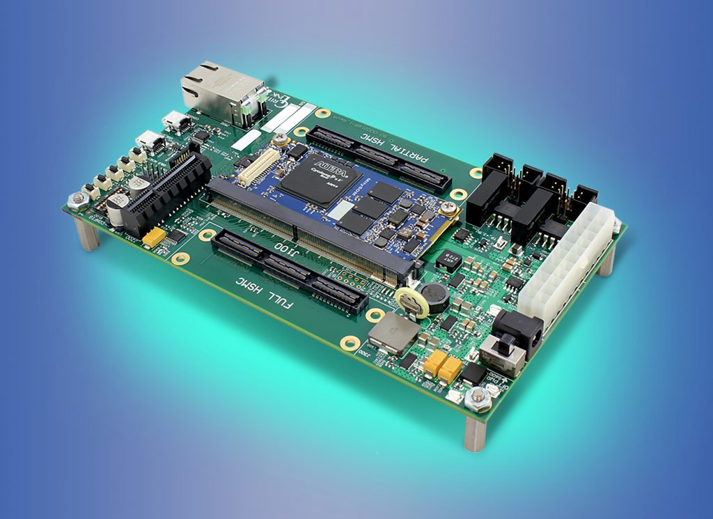
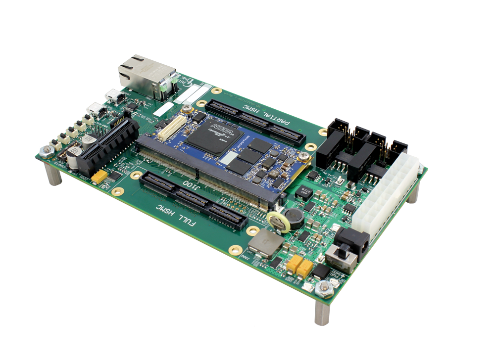
For developers requiring other cameras or sensors, Critical Link will also raffle one of its standard MitySOM-5CSx Development Kits. The kit is intended for development of any embedded electronics application, including embedded imaging. It features an array of interfaces and expansion headers such as USB, Debug RS232 to USB Console, Full HSMC Expansion Connector, Partial HSMC Expansion Connector, PCI-e x4 Expansion Header, MMC/SD Card, Gigabit Ethernet and Dual CAN Bus interfaces.
The company will also be demonstrating two recently released technologies: the MityCAM-C50000 and the MitySOM-A10S Image Processing Board. The MityCAM-C50000 system is an evaluation platform for the CMV50000 high speed image sensor from ams / CMOSIS, with 47.5MP resolution running at 30 frames per second, and multiple interfaces including USB3 Vision® and HDMI preview as standard, with custom options to include CoaXPress, Camera Link, GigE Vision, and others.
The MitySOM-A10S Image Processing Board is an open architecture design featuring dual core Cortex-A9 ARMs with up to 480KLE user-programmable FPGA fabric, DDR4 memory, and 12 high-speed transceiver pairs. It is an ideal solution for machine vision and scientific imaging applications. Both the MityCAM-C50000 and MitySOM-A10S support OpenCL™ and high-level synthesis (HLS) tools for accelerating design cycles and targeting C/C++ code to the FPGA, and provide unparalleled ease of customization for complex imaging platforms.
As the leading event for OEMs developing scientific and industrial imaging systems, Photonics West draws attendees working in areas of biomedical, test & measurement, unmanned systems, energy & utilities, and many others. Critical Link’s System on Modules and Embedded Imaging Platforms are designed for industrial performance applications across these areas, ensuring a faster time to market, lower development costs, and long-term availability.
All products mentioned here are available from Critical Link and selected partners, beginning January 2019. Please visit www.criticallink.com or email info@criticallink.com to learn more.
About Critical Link Syracuse, N.Y.-based Critical Link (www.criticallink.com) is an embedded systems engineering firm offering customizable system-on-modules (SOMs) and imaging platforms for industrial, medical, scientific, and defense applications. Critical Link’s end-to-end product engineering services include design, development, and production. Critical Link is a premier Partner in the Imaginghub by Basler, a Platinum Member of the Intel (Altera) FPGA Design Solutions Network and the Intel IoT Solutions Alliance, and is ISO 9001:2015 Registered by SRI Quality System Registrar.
Company will showcase new technologies for industrial embedded imaging at SPIE Photonics West 2019, Moscone Center, San Francisco, Feb. 5 – 7, in South Hall booth #240.
Syracuse, N. Y. – Critical Link, a leading provider of electronics and engineering services for industrial embedded imaging applications, will showcase two new technologies at Photonics West 2019, the world’s largest photonics technologies event.
The first, the MityCAM-C50000, is an imaging system specially designed as an evaluation platform for the CMV50000 high-speed image sensor from ams / CMOSIS. The global shutter sensor features 47.5MP resolution at 30 frames per second, mono and RGB color options, with low dark noise and high dynamic range. The innovative system provides multiple interfaces including USB3 Vision® and HDMI preview as standard, with custom options that include CoaXPress, Camera Link, GigE Vision®, and more.
The powerful MityCAM-C50000 is an open architecture design that utilizes Critical Link’s other new technology, the MitySOM-A10S image processing board. This system on module (SOM) family features dual core Cortex-A9 ARMs with up to 480KLE user-programmable FPGA fabric, DDR4 memory, and 12 high-speed transceiver pairs, making it an ideal solution for machine vision and scientific imaging applications. The board is available in two configurations: first as a stack-through board for use in camera designs, and second with bottom-side, rugged board-to-board connectors for integration with an industrial baseboard.
Both the MityCAM-C50000 and MitySOM-A10S support OpenCL™ and high-level synthesis (HLS) tools for accelerating design cycles and targeting C/C++ code to the FPGA. The processor board runs embedded Linux out of the box and provides unparalleled versatility and ease of customization for complex imaging platforms.
As the leading event for OEMs developing scientific and industrial imaging systems, Photonics West draws attendees working on next generation designs in areas of biomedical, test & measurement, unmanned systems, energy & utilities, and many others. Critical Link’s SOMs and embedded imaging platforms are designed for next-generation performance in a variety of scientific, industrial, medical, and defense applications to ensure a faster time to market, lower development costs, and long-term availability.
The MityCAM-C50000 and MitySOM-A10S are available from Critical Link and select partners starting in January 2019. To see a demonstration of this remarkable new embedded imaging platform, please visit SPIE Photonics West 2019, Moscone Center, Feb. 5 – 7, South Hall booth #240. For more information, please go to www.criticallink.com or email us at info@criticallink.com.
About Critical Link
Syracuse, N.Y.-based Critical Link (www.criticallink.com) is an embedded system engineering firm providing system on modules (SOMs) and embedded imaging solutions for industrial performance applications. The company’s expertise in image sensor integration, system-on-chip (SoC) and field-programmable gate array (FPGA) designs, vision protocols, and signal processing has made it a leader in board-level solutions and custom designs for OEMs and embedded developers around the world. Critical Link is a Platinum Member of the Intel (Altera) FPGA Design Solutions Network and the Intel IoT Solutions Alliance, and is ISO 9001:2015 Registered by SRI Quality System Registrar.
Machine vision systems have traditionally consisted of stand-alone cameras tethered to PC-based boards or frame grabbers using highspeed interfaces such as Camera Link, CoaXPress and Gigabit Ethernet. By transferring this data to host computer memory, off-the-shelf software can be used to analyze the captured images and extract information or make a pass/fail decision. While such systems are effective, they generally rely on a very expensive and space-consuming host computer to perform much of the image processing.
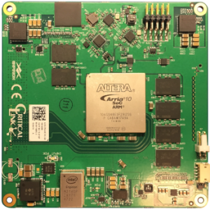
Figure 1: (a) Critical Link’s MitySOM-A10S is an Intel/Altera Arria 10 SoC board that features dual core ARM and FPGA fabric, on-board power supplies, two DDR4 RAM memory subsystems, a micro SD card, optional eMMC, on-board RTC, a USB port, and temperature sensors. (b) The MitySOM-A10S development kit provides everything needed to initiate your embedded development project, and includes external interfaces such as USB, FMC expansion connectors, PCI-e expansion headers, and Gigabit Ethernet.
Most commonly, image processing algorithms are implemented using off-the-shelf software packages such as HALCON from MVTec and MATLAB from Mathworks. In recent years, there has been a growing demand to perform preprocessing on the image data before it is transferred from the camera to the PC. As a result, many of today’s cameras feature on-board FPGA fabric to perform such functions as Bayer interpolation, image enhancement, and noise reduction directly on the cameras themselves.
While adding an FPGA to the camera introduces additional capability, it does not address the never-ending push to reduce the size, weight and power (SWaP) and recurring cost of imaging and machine vision systems, particularly applications such as portable medical instrumentation, robotics, sensory augmentation systems, and unmanned aerial vehicles. To achieve dramatically lower cost and SWaP, alternatives to PC-based systems must be considered.
ALTERNATIVE APPROACHES
In the past, designers needing to eliminate the PC have had the option to either develop a complete “smart camera” from scratch or use an off-the-shelf camera with custom-developed embedded processor/ FPGA boards to host the image processing software. Both of these options require extensive schedule and engineering resources to develop, and can be expensive to produce if volumes are not high.
The advent of the System on Module (SOM) has allowed a third option, which is to select an off-the-shelf processor board (the SOM) and develop simplified interface boards to connect cameras designed with off-the-shelf modules or custom-designed sensor boards. Such SOMs typically contain one or more processors (RISC or DSP, or both), FPGA fabric, RAM, and I/O capability, while supporting multiple operating systems. SOMs are small (2” × 3” for example), so they can fit into small form factor industrial cameras. An interface board is then used to connect the SOM to external interfaces such as PCI, Gigabit Ethernet, USB3, and CAN Bus.
The cost of developing a SOM-based system is significantly lower than that of developing a complete camera/processor system, since the most complex aspects of design and layout have already been performed and tested by the SOM manufacturer. Then, the interface board design generally requires much lower design effort, especially when using pre-existing development board schematics and design files as a starting point, which some SOM suppliers make available. Furthermore, the SOM supplier manages parts procurement and component obsolescence for the SOM, eliminating maintenance and support responsibilities for the camera designer for the lifespan of the product.
One example of such a SOM is Critical Link’s MitySOM-A10S, an Intel/Altera Arria 10-based board that features up to 480KLE FPGA fabric, onboard power supplies, two DDR4 RAM memory subsystems, a micro SD card, optional eMMC, on-board RTC, a USB 2.0 port, and temperature sensors (Figure 1). With an Arria 10 SX processor that features dual-core Cortex-A9 32-bit RISC processors with dual NEON SIMD coprocessors, the multiprocessing unit (MPU) is capable of running any number of commercial operating systems, bare metal, and embedded Linux.
PARALLEL DEVELOPMENT
It is common for SOM suppliers to offer development kits that include a full-featured base board with multiple interfaces such as USB2, USB3, RS-232, FMC expansion connectors, PCI-e expansion headers, Gigabit Ethernet, HDMI, and CAN Bus. Some suppliers have started offering development kits specifically for embedded imaging projects that feature popular machine vision sensors. Regardless of which kit is selected, using an off-the-shelf development kit means that software and hardware development can occur in parallel, which can drastically speed time to market.
Figure 2: The embedded vision development kit uses a MitySOM-5CSx Module with an interface board. The development kit enables rapid prototyping and provides an open architecture for developers to embed off-the-shelf IP or their own proprietary image processing algorithms.
Development kits give hardware designers the option to use manufacturer-provided schematics and design files as a starting point to test out the validity of their designs before committing to their custom interface board. As hardware engineers develop the necessary interfaces, software engineers can choose from numerous commercial and open source image processing libraries to develop the final product. One such library is the Video Image Processing (VIP) suite from Intel, a library of FPGA intellectual property (IP) that includes such functions as color space conversion, up/down image scaling, frame rate conversion, image convolution, video I/O formatting, and thresholding.
Other off-the-shelf packages include Mathwork’s Image Processing Toolbox that provides a set of algorithms for image segmentation, enhancement, noise reduction, geometric transformations, image registration, 3D image processing and HALCON from MVTec that offers FPGA RTL export of the software’s image processing libraries.
PROGRAMMING FPGAS
Although the idea of using an FPGA for image processing can be daunting without the right experience, new tools exist to make such development easier. To program the numerous system logic elements, registers, memory blocks, and multiplier/accumulators that comprise the FPGA fabric of these devices, developers can use software such as Intel’s Quartus Prime. This enables analysis and synthesis of hardware description languages (HDLs) such as VHDL and Verilog to describe the structure and behavior of digital logic circuits.
Once written in an HDL, the design can be compiled, timing analysis performed and the on-board processors and FPGA configured to perform the required function. Quartus Prime, for example, includes an implementation of VHDL and Verilog for hardware description and visual editing of logic circuits.
A number of development tools are available to speed up the programming of such devices for image processing and machine vision applications. One approach would be to use Open Computing Language (OpenCL), a framework for writing programs that executes across CPUs, GPUs, DSPs and FPGAs. Using this method, a programmer would write code in C/C++ and test and validate the code on a PC. Once verified, processing kernels can be recompiled to register-transfer level (RTL) and dispatched to FPGA gate logic.
A similar approach would involve using the Open Source Computer Vision Library (OpenCV), a C++-based open source computer vision and machine learning software library for computer vision applications. OpenCV has more than 2,500 libraries of algorithms used to detect and recognize faces, identify objects, classify human actions in videos, track camera movements, track moving objects, extract 3D models of objects, and produce 3D point clouds from stereo cameras.
A more advanced approach, however, involves high-level synthesis (HLS), also known as C synthesis. With this method, code written in C/C++ or MATLAB is analyzed and transcompiled into a hardware description language (such as VHDL) which is, in turn, synthesized to the gate level using a logic synthesis tool.
Both OpenCL and HLS usually result in a substantial reduction in implementation time since the software is easier to write and, more importantly, iteration and/or modification can be more easily performed.
EMBEDDED IMAGING DESIGN
While FPGAs perform pipelined functions very efficiently and quickly, there are limitations to FPGA-only based designs. Functions such as high/low pass, thresholding, and Bayer transformations can be partitioned to the FPGA. However, others that require the complete image to be iteratively analyzed may be better suited for running on an embedded CPU or GPU.
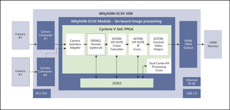
As an example, the Dart board level camera series from Basler features an FPGA on the sensor board that does fixed image pre-processing. Beyond that, advanced image processing and analytics would have to be performed outside the camera’s FPGA. This is performed using a SOM module, which is included in the Dart’s embedded vision development kit (VDK) (Figure 2).
Figure 3: Fixed pre-processing functions provided by the sensor board’s FPGA include noise reduction, white balancing, de-Bayering, and an edge detection algorithm (shown here, on left) which runs onboard a SOM without the support of a PC.
The VDK consists of the Basler Dart camera module, an LVDS cable connection to an interface board which features HDMI, Ethernet, USB 2.0, and GPIO output, and a SOM. Image preprocessing functions such as Bayer conversion, bad pixel correction and noise reduction take place on-board the camera module. This leaves developers free to use the SOM’s on-board ARM and FPGA fabric for their own image processing functions (Figure 3).
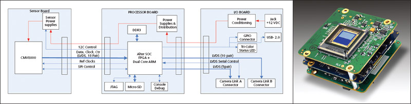
This modular concept of sensor board, processor board, and interface board is taken a step further with Critical Link’s MityCAM architecture. Figure 4 shows a block diagram of a three-board system where each board allows for a certain level of interchangeability depending on the requirements of the system. CMOS and CCD sensor boards are available with an array of image sensors from top manufacturers, and new sensors can be integrated quickly and cost effectively.
Figure 4: (a) Block diagram of Critical Link’s MityCAM architecture, a three board system that features an array of CMOS and CCD sensor options, two processor boards with ARM & FPGA fabric open for user programming, and interchangeable interface boards with options for Gigabit Ethernet, USB3, USB2, Camera Link, CoaXPress, and HDMI. (b) An example of a 3-board camera system in its stacked configuration.
The central processing board provides options based on SOMs, both of which feature ARM and FPGA fabric in an open architecture for developers to embed their selected image processing functions. Interface boards can be selected with dual Camera Link, USB3, Gigabit Ethernet, HDMI, USB2, and CoaXPress. Regardless of the individual board selected, the system can be arranged in a stack that uses strong board-to-board connectors, and is available in production volume with or without mechanical packaging.
While embedded imaging and machine vision systems programming may initially appear complex, the number of hardware and software development tools now available are making these development cycles faster and more cost-effective. In applications such as portable instrumentation, autonomous systems, and process automation equipment, embedded systems will reduce the size, weight and power required and the upfront investment of both schedule and engineering resources.
The new MityCAM-C50000 platform serves as the evaluation kit for the CMV50000 image sensor from ams / CMOSIS, and can jump-start embedded system development.
Syracuse, N. Y. – Critical Link, a leader in embedded electronics solutions, announces its latest embedded imaging solution, the MityCAM-C50000. The new MityCAM-C50000 serves as the official evaluation platform for the CMV50000 CMOS image sensor from ams / CMOSIS. The global shutter sensor features 47.5MP resolution (7920 pixels x 6004 pixels) at 30 frames per second, with mono and RGB color options, low dark noise, and high dynamic range. The sensor outputs in subLVDS mode and provides special capabilities in binning, subsampling, and on-chip corrections.
“The performance of the CMV50000 sensor is unparalleled for machine vision and video applications,” notes Omar Rahim, vice president of imaging products at Critical Link. “We are pleased to have been selected by the ams team to develop this evaluation kit. The CMV50000 sensor and the MityCAM-C50000 platform are enabling innovation on factory floors, in healthcare, and numerous other areas.”
The MityCAM-C50000 provides multiple interfaces including USB3 Vision® and HDMI preview as standard, with custom options to include CoaXPress, Camera Link, GigE Vision®, and others.
The system is based on an open architecture embedded processing design utilizing Critical Link’s MitySOM-A10S image processing board. The board features Intel’s Arria 10 SoC with dual core Cortex-A9 ARMs and up to 480KLE user-programmable FPGA fabric, DDR4 memory, and 12 high-speed transceiver pairs, making it an ideal solution for embedded vision and scientific imaging applications.
Mr. Rahim adds, “For many, the idea of programming an FPGA can be daunting. Today, however, new tools are making development easier and faster for image processing and machine vision applications.”
The MityCAM-C50000 architecture supports a number of development tools, including OpenCL™ and high-level synthesis (HLS). This ensures that anyone who can code in C/C++ is able to work with the FPGA. OpenCL also enables software acceleration, generating significant improvement in application speed.
Customers interested in the MityCAM-C50000 for evaluation of the CMV50000 sensor may connect with their local ams representative, or contact Critical Link via info@criticallink.com. Developers designing a custom system around the CMV50000 are encouraged to contact Critical Link before getting started to obtain design files and other helpful information. Critical Link’s engineering team is also available to assist with new development projects or customization of the MityCAM-C50000 design.
Syracuse, N.Y.-based Critical Link (www.criticallink.com) is an embedded system engineering firm providing system on modules (SOMs) and embedded imaging solutions for industrial performance applications. The company’s expertise in image sensor integration, system-on-chip (SoC) and field-programmable gate array (FPGA) designs, vision protocols, and signal processing has made it a leader in board-level solutions and custom designs for OEMs and embedded developers around the world. Critical Link is a Platinum Member of the Intel (Altera) FPGA Design Solutions Network and the Intel IoT Solutions Alliance, and is ISO 9001:2015 Registered by SRI Quality System Registrar.
SYRACUSE, N.Y. – Critical Link, LLC is pleased to announce the company’s recent recognition as a 2018 Economic Champion, as selected by Centerstate CEO. Each year Centerstate CEO recognizes the region’s outstanding businesses and organizations as Economic Champions for their contributions, including expanding their employee base, making capital investments due to growth, and receiving local, statewide, or national awards.
This recognition follows on the heels of a number of other awards received by Critical Link this year, including most recently being one of only five electronics engineering companies named to the 2018 Inc. 5000 Fastest Growing Companies List. In addition, Critical Link was selected by Embedded Advisor magazine as one of the Top 20 Electronics Design & Solutions Providers, as well as presented with a Bronze-level Innovator Award from Vision Systems Design for one of our latest embedded imaging product developments.
According to John Fayos, Co-Founder and President at Critical Link, “In the last few years Critical Link has experienced significant growth, both in overall revenue and in new product sales. 2017 delivered the best performance of the company’s 20-year history — with a 56% year-over-year increase in revenue led by triple digit growth in product sales. For 2018 we expect to build further on that growth with an additional increase of more than 10%.”
The company’s tremendous growth in product sales is being driven by recent investments in research & development, as well as a number of significant contract wins including one with a new customer located in France. This customer selected Critical Link as a key partner to help them design and deliver industrial machine vision inspection systems to one of the world’s top electronics manufacturers. In under 6 months Critical Link designed a custom electronics package, built prototypes, developed and tested software, and successfully delivered the first order of 1,100 units.
“The company’s successful performance on this contract is a testament to our capabilities as both an engineering design house and a worldwide supplier of production-ready solutions,” said Fayos.
For more information on Critical Link’s products or capabilities, visit www.criticallink.com.
ABOUT THE COMPANY:
Critical Link, LLC (Syracuse, NY; www.criticallink.com) develops embedded systems solutions, system on modules (SOMs), and imaging hardware for industrial electronic applications. The company provides expertise in image sensor technology, system on chip (SoC) and field-programmable gate array (FPGA) design, signal processing, and vision protocols for product development through production.
Privately held, Critical Link is a Platinum member of the Intel FPGA Design Services Network and Intel IoT Solutions Alliance, a Platinum member of the Texas Instruments Design Network, and a certified member of the Arrow Consulting Engineering Services (ACES) program.
SYRACUSE, N. Y. – Critical Link, LLC experts in embedded systems, system on modules (SOMs), and imaging systems for electronic applications, has been selected as one of Inc. Magazine’s 5000 fastest-growing, privately-held companies in America for 2018. With 2017 revenues of $11.7 million and the company’s extraordinary 76% growth rate over the past 3 years, Critical Link has earned the No. 4366 spot on this prestigious list of North American entrepreneurs.
John Fayos, Critical Link’s president, notes, “I’m incredibly proud of the strides we’ve made in the increasingly competitive SOM market. Our reputation as a provider of high-quality, long-lifespan embedded electronics has driven growth with industrial, commercial, and medical customers around the world.”
Critical Link is one of four embedded electronics companies on the 2018 Inc. 5000 list, and the only embedded electronics company that provides off-the-shelf board level solutions. The company specializes in system on chip (SoC), image sensor integration, field-programmable gate array (FPGA) designs, vision protocols, and signal processing.
Critical Link’s remarkable growth is due, in part, to pioneering innovative embedded systems technology and products, such as the recently introduced MitySOM-A10S-DSC processor board for the next generation of embedded imaging applications.
Highly-configurable with dual-side connectors (DSC) for stack-through construction, the advanced system on module is built around the Intel®/Altera Arria® 10 SoC processor with dual core ARM. The company’s new A10S-DSC board is ideal for applications in industrial instrumentation, test and measurement, medical imaging, robotics, process automation and control and more. To learn more about Critical Link’s MitySOM-A10S-DSC, please visit: https://www.criticallink.com/product/mitysom-a10s-dual-side-connectors/.
For more information about the company’s custom imaging design, product development, and full lifecycle engineering support services, please go to: https://www.criticallink.com/services/.
While this is the first time Critical Link has made the list, it’s seen continuous growth since it was founded by four former Sensis employees in 1997. The company is poised to continue its growth with projected 2018 revenue of $13M. Critical Link’s sustained success is in large part attributed to a shift in focus—from services to products.
“For most of our history we’ve primarily been an engineering services firm,” Fayos explains. “In 2004 we made a strategic business decision to enter into the product space. It’s taken some time, but today about 75% of Critical Link’s revenue comes from our embedded board products.”
The MitySOM-A10S
The company recently announced the launch of its latest design—the MitySOM® A10S System on Module which is built around the Intel/Altera Arria® 10 SoC processor for industrial applications. Although general availability won’t be until this fall, Critical Link is already seeing traction with customers in process automation, medical imaging, industrial robotics, and more.
ABOUT THE COMPANY:
Critical Link, LLC(Syracuse, NY www.criticallink.com), founded in 1997, develops embedded systems solutions, system on modules (SOMs) and imaging systems for a wide variety of electronic applications. As experts in image sensor technology, system on chip (SoC) and field-programmable gate array (FPGA) design, signal processing, and vision protocols, we support all product development tasks, from concept to final production.
Our flexibility allows us to deliver full lifecycle support and services at any step along the product development path. From hardware, firmware, and software development, to prototyping and manufacture/assembly, Critical Link is committed to helping our OEM customers reach their project goals quickly and cost-effectively.
Privately held, Critical Link is a Platinum member of the Intel FPGA Design Services Network and Intel IoT Solutions Alliance, and a certified member of the Arrow Consulting Engineering Services (ACES) network.
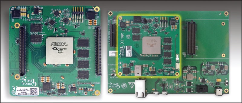
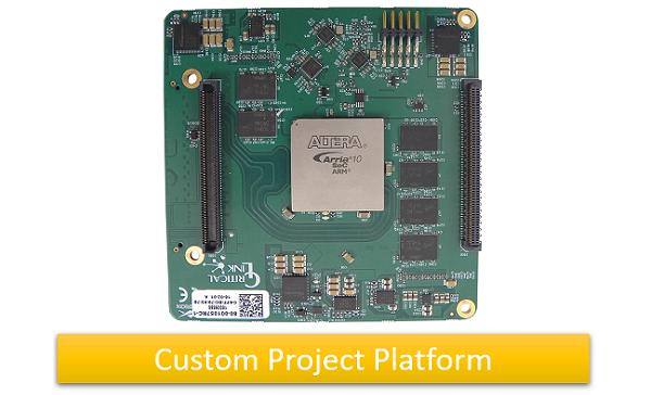
The new Arria 10 SoC board-level solution features dual-side connectors making it ideal for industrial camera designs with advanced image processing requirements.
SYRACUSE, N. Y. – July 18, 2018 – Critical Link, LLC, experts in image sensor integration, system-on-chip (SoC) and field-programmable gate array (FPGA) designs, vision protocols, and signal processing, introduces the MitySOM-A10S-DSC processor board for the next generation of embedded imaging applications. The new board features dual-side connectors for stack-through configurations. It is a highly-configurable system-on-module (SoM) featuring the Intel®/Altera Arria® 10 SoC with dual core ARM and up to 480KLE FPGA fabric. The module includes on-board power supplies, two DDR4 RAM memory subsystems, and a rich set of user interfaces.
The A10 board supports both OpenCL™ and high-level synthesis (HLS) tools for accelerating design cycles and targeting C/C++ code to the FPGA. Critical Link’s innovative MitySOM-A10S-DSC processor with embedded Linux provides operating system support, versatility, and ease of customization for complex imaging platforms.
Applications include machine vision, test and measurement, embedded instrumentation, industrial automation and control, and industrial and medical instrumentation. Critical Link successfully demonstrated a 50MP imaging platform with on-board processing using the MitySOM-A10S-DSC at several trade shows this year, including SPIE Photonics West, AIA Vision, and SPIE Defense & Commercial Sensing. The company is currently developing a series of image sensor boards and interface boards for use with the innovative MitySOM-A10S-DSC platform which will support a wide range of vision protocols including GigE Vision, USB3 Vision, and Camera Link.
Critical Link, LLC(Syracuse, NY www.criticallink.com), founded in 1997, develops embedded systems solutions, system on modules (SOMs) and imaging systems for a wide variety of electronic applications. As experts in image sensor technology, system on chip (SoC) and field-programmable gate array (FPGA) design, signal processing, and vision protocols, we support all product development tasks, from concept to final production.
Our flexibility allows us to deliver full lifecycle support and services at any step along the product development path. From hardware, firmware, and software development, to prototyping and manufacture/assembly, Critical Link is committed to helping our OEM customers reach their project goals quickly and cost-effectively.
Privately held, Critical Link is a Platinum member of the Intel FPGA Design Services Network and Intel IoT Solutions Alliance, and a certified member of the Arrow Consulting Engineering Services (ACES) network.
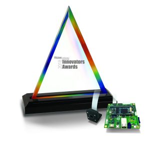
The company was honored with the Innovators Award – Bronze Level from Vision Systems Design (VSD) at a special ceremony on April 10, 2018, in Boston, Mass.
Critical Link, LLC, experts in image sensor technology, system-on-chip (SoC) and field-programmable gate array (FPGA) designs, vision protocols, and signal processing, received the prestigious Innovators Award – Bronze level at the Fourth Annual Vision Systems Design Innovators Awards presentation, held during The Vision Show in Boston, Mass.
The MitySOM®-5CSX Embedded Vision Development Kit (VDK) for Basler dart BCON Cameras was selected for the award in the Embedded Vision category by a panel of esteemed experts from system integrator and end-user companies. Critical Link’s Embedded Vision Development Kit provides a complete hardware and software solution for system developers, streamlining embedded imaging application developments.
The kit includes on-board image processing capabilities with FPGA fabric and dual core ARMs, and rapid prototyping via Altera’s VIP Suite and OpenCL. It also comes with a variety of sensor options and communication interfaces, and includes complimentary access to Basler’s intuitive Pylon camera software suite.
The Innovators Awards are judged based on the following criteria:
Originality
Innovation
Impact on designers, systems integrators, end users
Fulfilling a need in the market that hasn’t been addressed
Leveraging a novel technology
Amber Thousand, director of marketing for Critical Link, notes, “Our MitySOM Embedded VDK engineering team is honored to be selected as an Innovators Awards recipient for 2018. Our out-of-the-box kit comes complete with the MitySOM-5CSX module, camera(s), and necessary cabling to start a project, making it easier and faster than ever to bring an embedded vision product to market. We are delighted to have our product innovation acknowledged by this distinguished award from Vision Systems Design”.
The team leader of embedded module business at Americas at Basler,Tim Coggins, remarks, “The Critical Link engineering team amazed us by integrating an early prototype of the Basler BCON LVDS module before anyone else. Their knowledge and integration capabilities are first rate. The MitySOM Embedded Vision Development Kit is a great product for the embedded design engineering community, providing rapid prototyping and a fast path to production. This award and recognition is very well deserved.”
To learn more about Critical Link’s embedded systems, custom imaging platforms, and full engineering support services and product development, visit http://www.criticallink.com/services/.
All 2018 Vision Systems Design Innovators Awards Honorees will be featured in the June issue of Vision Systems Design magazine as well as on http://www.vision-systems.com.
About the Company: Critical Link, LLC, founded in 1997, develops embedded systems solutions, system on modules (SOMs) and imaging systems for a wide variety of electronic applications. As experts in image sensor technology, system on chip (SoC) and field-programmable gate array (FPGA) design, signal processing, and vision protocols, we support all product development tasks, from
concept to final production.
Our flexibility allows us to deliver full lifecycle support and services at any step along the product development path, when and where needed, to effectively keep costs down. From engineering to hardware and software development, and mechanical engineering to prototyping and manufacture/assembly, Critical Link is committed to helping our OEM customers reach their project goals quickly and cost-effectively.
Privately held, Critical Link is a Platinum member of the Intel FPGA Design Services Network and Intel IoT Solutions Alliance, and is ISO 9001:2015 registered by SRI Quality Systems Registrar.
About The Vision Systems Design 2018 Innovators Award Program: The Vision Systems Design 2018 Innovators Award program reviewed and recognized the most innovative products and services in the vision and image processing industry. Honorees were announced at AIA Vision 2018 held in Boston, MA, USA. Criteria used in the Innovators Awards ranking included: originality, innovation; impact on designers, systems integrators and end-users; fulfilling a need in the market that hasn’t been addressed, leveraging a novel technology, and increasing productivity.Back in the day, a growing shortage of engineering resources threatened to hold back innovation and development initiatives in the realm of embedded hardware and software.

 Syracuse, N. Y. – Critical Link, a leading provider of electronics and engineering services for industrial embedded applications, will showcase its latest board-level solutions at






 The new Arria 10 SoC board-level solution features dual-side connectors making it ideal for industrial camera designs with advanced image processing requirements.

 Use our SOM Selector