Embedded.com is running excerpts from Embedded Computing for High Performance, the highly informative (and, yes, educational) book by João Cardoso, José Gabriel Coutinho, and Pedro Diniz. In my last post, I summarized the initial article, which focused on target architectures and multiprocessor and multicore architectures. This post covers core-based architectural enhancement and hardware accelerators.
In this excerpt, the authors address how CPUs have been further enhanced, beyond multicore, by incorporating more than one multicore CPU, integrated as a chip multiprocessor (CMP). They offer two ways in which CMPs can be organized.
The first is Single Instruction, Multiple Data (SIMD) units. These are:
…hardware components that perform the same operation on multiple data operands concurrently. Typically, a SIMD unit receives as input two vectors (each one with a set of operands), performs the same operation on both sets of operands (one operand from each vector), and outputs a vector with the results.
Intel microprocessors (MMX, SSE, AVX ISA extensions) have included SIMD units since the late 1990’s, and ARM got in the act more recently with SIMD extensions to ARM-Cortex (NEON technology.)
Typical tasks that SIMD units take care of are basic arithmetic and other operations, like square root. SIMD unit enhance performance by their ability to simultaneously load from and store to memory multiple data items, taking advantage of the entire width of the memory’s data bus.
One bit of advice the authors offer:
To exploit SIMD units, it is very important to be able to combine multiple load or store accesses in a single SIMD instruction.
The second option for organizing CMPs presented is Fused Multiply-Add (FMA) units.
Fused Multiply-Add (FMA) units perform fused operations such as multiply-add and multiply-subtract. The main idea is to provide a CPU instruction that can perform operations with three input operands and an output result.
Both Intel and ARM have microprocessors that include FMA.
Here the authors discuss two types of hardware accelerators, GPU accelerators and reconfigurable hardware accelerators (absolutely something we’re quite familiar with here at Critical Link).
GPU accelerators were initially used for graphical computation, but these days they also support additional application areas, including scientific and engineering apps. Then there’s our friend, the reconfigurable hardware accelerator:
Given the ever-present trade-off between customization (and hence performance and energy efficiency) and generality (and thus programmability), reconfigurable hardware has been gaining considerable attention as a viable platform for hardware acceleration. Reconfigurable devices can be tailored (even dynamically—at runtime) to fit the needs of specific computations, morphing into a hardware organization that can be as efficient as a custom architecture. Due to their growing internal capacity (in terms of available hardware resources), reconfigurable devices (most notably FPGAs) have been extensively used as hardware accelerators in embedded systems.
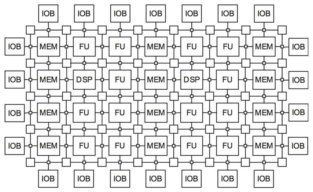
The authors give a shout out to components that combine FPGA and DSP. As I said, right up our alley. Here’s a block diagram of a reconfigurable fabric that includes both FPGA and DSP. It doesn’t look anything like the sort of block diagram we’d present to a client, but I had my reasons for including it here.

As with my earlier post, I encourage readers to head over to embedded.com to read the full excerpts (which are all accompanied by ample diagrams and other illustrations).
