Contact Critical Link for product availability
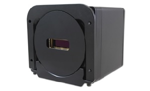
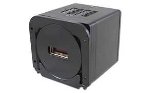
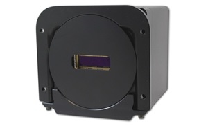
Overview
 Features
- Front-illuminated sensor
- Enhanced IR sensitivity
- No etaloning
- Large pixel size: 24 x 24 micron
- TE-Cooled to -15°C
Applications
- Raman Spectroscopy
- Low-light Imaging
- Industrial Inspection
- Semiconductor Inspection
- Portable Scientific Imaging
Documentation
MityCCD Family-level Documentation
- Binning and Read-out Modes
- Camera Performance
- Mechanical Drawings
- Sensor Selection
- Software
- SDK C Applications Programmer Interface – coming soon…
- MityCCD Viewer User’s Guide
Specifications
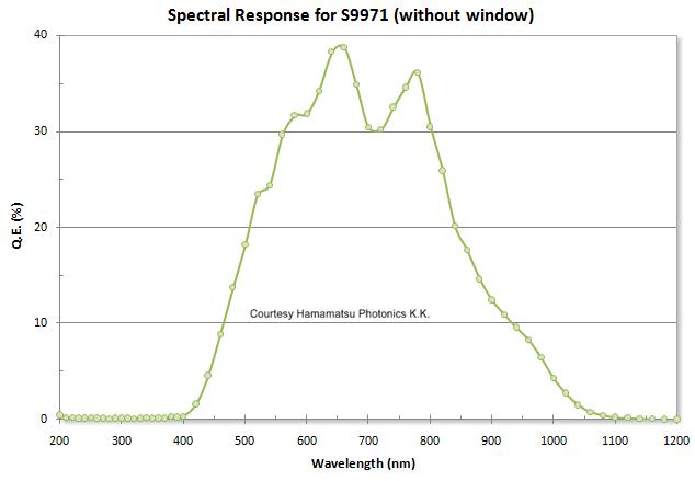
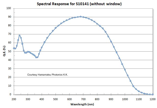
Sensor Specification
| Type | Front-illuminated |
| Pixel Size | 24 um x 24 um |
| Image Area | Various – See Camera Models Above |
| Pixel Array | Various – See Camera Models Above |
| Well Capacity |
240 ke¯ (typical – vertical)
|
| Well Capacity |
480 ke¯ (typical – horizontal)
|
| Dark Current |
100 e¯/pixel/sec (typ. @ 0 °C)
|
System Noise
| Noise (typ) |
TBD e¯ RMS @ 500KHz
|
Data Acquisition & Binning Modes
| Area Read |
Full image and sub-area (any rectangular region of the CCD)
|
| Full Binning |
Standard CCD binning (all CCD rows summed in read-out register)
|
| Partial Binning |
Some rows summed in CCD and partial results summed in MityDSP
|
| Area Mask Binning |
Vertical and horizontal binning in MityDSP
|
| Multiple Binning Patterns |
Multiple Binning patterns stored in memory and swapped in as directed on a cycle basis
|
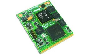
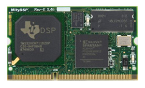
On-board Processor (MityDSP)
| CPU Engine |
Floating-point DSP, FPGA, FLASH, SDRAM (up to 32MB)
|
| Full Featured SDK |
Supports rapid application development
|
| Applications |
Peak finding, signature analysis, general purpose computing, etc.
|
Cooling
| Type |
Thermo-electric to -15 °C (from 20 °C ambient) +/- .1 °C
|
Mount
- Several standard mounts available – Contact Critical Link for more information.
Environment
| Temperature |
0°C to +50°C
|
| Humidity |
10% to 90% non-condensing
|
Electrical
| Voltage |
110V / 220V or 12-24 VDC
|
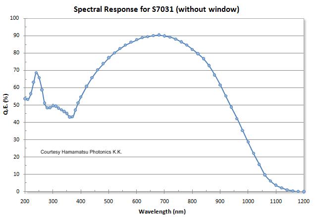
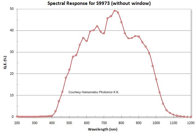
Quantum Efficiency
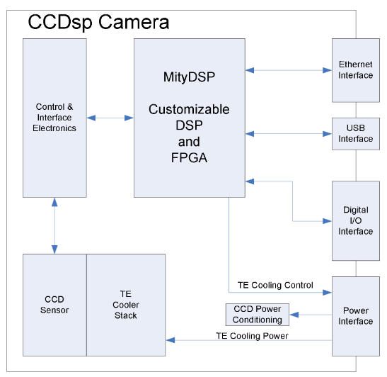
Block Diagram
Interfaces
| USB | Supports USB 2.0 |
| Ethernet |
Supports full TCP / UDP stack over 10 / 100 Base T
|
| Digital I/O |
Supports external triggering and control of outboard devices
|
Mechanical
| Dimensions |
98mm x 100mm x 90mm (3.86″ x 3.94″ x 3.54″)
|
| Weight |
750g (26oz.)
|
Development Tools and Software
Purchase
| Camera Model | Image Area | Active Pixels | Buy | ||
| Width (mm) | Height (mm) | Horizontal | Vertical | ||
| MityCCD-H9973-1007 | 24.576 | 2.976 | 1024 | 124 | Buy |
| MityCCD-H9973-1008 | 24.576 | 6.048 | 1024 | 252 | Buy |
Find your local sales contact.
*Note: Contact Critical Link for ordering information.