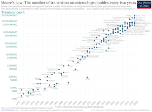
There’s always something more to say on Moore’s Law, and several writers are saying it in a series of pieces on EE Times.
It seems that Moore’s Law, which holds that the number of transistors in an integrated circle doubles roughly every couple of years, can’t keep up with the times. Not that the nearly 60-year-old observation by Gordon Moore was ever a law to begin with, just a rule of thumb. But it has held up fairly well over the years. It’s just that there’s been such an unprecedented demand placed on chips – a demand that I doubt Moore foresaw in 1965 when he coined his term – that the scaling that Moore’s Law observed and predicted would continue is running into a wall. The “scaling is stalling.”
With each successive iteration, chip shrinking takes longer and costs more. As chipmakers and systems strive to continue driving advancements in power, performance, area, cost, and speed to market, new design and production paradigms are required. (Source: EE Times)
Power, performance, area, cost and speed to market. Is that all???
Anyway, as authors Maurizio Di Paolo Emilio and Stefani Munoz write, those “new design and production paradigms are on their way.”
The next revolution in advanced packaging provides a major improvement over conventional multi–chip packaging techniques, with the substrate’s wiring used to complete the electrical interconnections between chips. Each successive technology offers higher I/O density, as well as lower power consumption per bit of data transfer.
Nirmalya Maity, a VP with Applied Materials, contributed a piece on advanced packaging approaches that support heterogeneous design and integration to yield improvements in PPACt. (This is Applied Materials’ acronym for power efficiency, performance, area, cost, and time to market.) In his piece, Maity discusses how engineers are using a heterogenous approach that lets them break a large design into smaller pieces – chiplets – that can be tied into a single package.
One approach to bring chiplets together is through 3D stacking using through–silicon vias (TSVs). 3D interconnects similar to TSVs can be much shorter than conventional wiring, enabling lower power consumption and higher I/O density.
For example, compared with conventional bump–to–PCB connections, TSVs can increase I/O density by approximately 100× and reduce energy–per–bit transfer by approximately 15× depending on architecture and workload, thus enabling power–efficient 3D die stacking. Performance can also be increased as logic and memory are brought into closer proximity. (Source: EE Times – Maity)
What does Maity see coming next on the packaging front: hybrid bonding.
Hybrid bonding connects chips and wafers with direct copper–to–copper bonding, which reduces wiring distances and further increases I/O density to improve power efficiency and system performance. Compared with TSVs, hybrid bonding will enable another 10× increase in I/O density and another 2× improvement in energy per bit.
Another promising area is silicon photonics. Once used almost exclusively in the realm of high-end (low volume) systems, such as military applications, it’s making its way into consumer markets as well. Next gen silicon photonics platforms can stand up to the high bandwidth requirements of applications that use AI and machine learning – technologies that are increasingly finding a home in the “everyday” applications we all rely on.
More on silicon photonics later.
Suffice it to say that there’s a lot going on to keep Moore’s Law alive and well. (Maybe even for another sixty-plus years? Who knows?)
