Google is always up to something interesting, and one of the interesting things they’ve been up to is using Artificial Intelligence (AI) to automate the chip design process. The first place they’re deploying their new model is to design their next-gen tensor processing units (TPUs). These are the processors, used in Google’s data centers, that are tasked with increasing the performance of AI apps. So, AI deployed to help accelerate AI.
The [Google] researchers used a dataset of 10,000 chip layouts to feed a machine-learning model, which was then trained with reinforcement learning. It emerged that in only six hours, the model could generate a design that optimizes the placement of different components on the chip, to create a final layout that satisfies operational requirements such as processing speed and power efficiency. (Source: ZDNet)
Six hours, eh? That’s fast!
The specific task that Google’s algorithms tackled is known as “floorplanning.” This usually requires human designers who work with the aid of computer tools to find the optimal layout on a silicon die for a chip’s sub-systems. These components include things like CPUs, GPUs, and memory cores, which are connected together using tens of kilometers of minuscule wiring. Deciding where to place each component on a die affects the eventual speed and efficiency of the chip. And, given both the scale of chip manufacture and computational cycles, nanometer-changes in placement can end up having huge effects. (Source: The Verge)
This is the sort of work that could take engineers months to accomplish when done manually.
Optimizing chip layouts is a complex, intricate process. Processors contain millions of logic gates (standard cells), and macro (memory) blocks in the thousands. The “floorplanning” process that decides where to put the standard cells and macro blocks is critical, impacting how rapidly signals can be transmitted. Figuring out where to put the macro blocks comes first, and there are trillions+ of possibilities. Google researchers state that “there are a potential ten to the power of 2,500 different configurations to put to the test.” And given that Moore’s Law still seems to be with us – you remember Moore’s Law: the number of transistors on a chip doubles every year – there are ever more combinations to worry about.
Obviously, no one’s putting trillions of configurations to the test. Engineers rely on experience and expertise to create their floorplans. But AI can evaluate many different options, and no doubt come up with ones that even the best engineers might have missed.
Once the macro blocks are in place, the standard cells and wiring are added. Then there’s the inevitable revising and adjusting iterations. Using AI in this process is going to free up engineers to focus on more custom work, rather than having to spend their time on how to take care of component assembly.
The acceleration of chip design is not going to immediately solve the chip shortage crisis, which is at the fab rather than the design level. Still, over time, if next gen chips can be designed faster, it should have positive impacts throughout the supply chain.
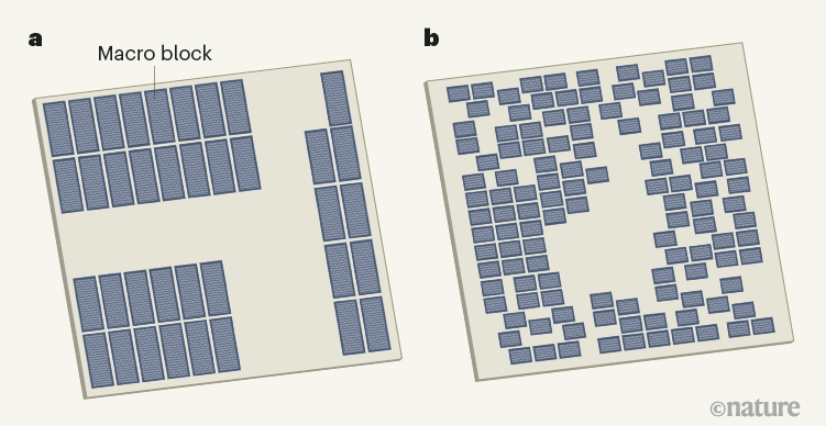
One of the most fascinating revelations was that the floorplan created by AI (that’s “b”, to the right) looks more random and scattershot than the very neat and orderly layout (“a” on the left) created by a human engineer. (This illustration is from Nature, which published a paper on the Google AI work.)
Inevitably, when we see AI being deployed, we ask ourselves whether AI, robots, machine learning will replace us humans.
Personally, I’m pretty sure that human engineers are still good for a while. There will always be work for engineers in a world that increasingly relies on technology in just about every aspect of our lives. There’s no denying that AI is going to take on some of the tasks that traditionally have been in human hands, but who knows what new opportunities this will create for knowledgeable and highly-skilled engineers like the ones we have here at Critical Link. Oh, brave new world!